AH103A Ver la hoja de datos (PDF) - WJ Communications => Triquint
NГғmero de pieza
componentes DescripciГіn
Fabricante
AH103A Datasheet PDF : 6 Pages
| |||
AH103A
High Gain, High Linearity ВҢ-Watt Amplifier
The Communications Edge TM
Product Information
Product Features
Product Description
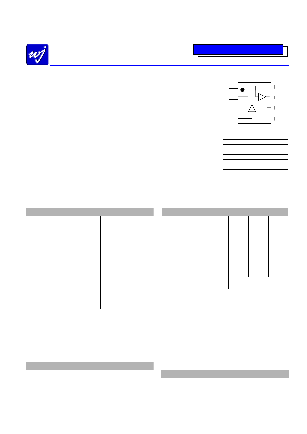
Functional Diagram
вЂұ 60 – 2700 MHz
вЂұ +27 dBm P1dB
вЂұ +46 dBm Output IP3
вЂұ 29 dB Gain @ 900 MHz
The AH103A is a high gain, high linearity ВҢ-Watt
amplifier. This device is comprised of two individual
MMIC amplifiers internally and can be used with an
external interstage match for any of the mobile
infrastructure frequency bands. The dual-stage
вЂұ Excellent ACPR
вЂұ MTTF > 100 Years
amplifier achieves up to +46 dBm IP3 performance
with 29 dB gain.
вЂұ Lead-free/green/RoHS-compliant The device conforms to WJ Communications’ long
SOIC-8 Package w/ heat slug history of producing high reliability and quality
components. The AH103A has an associated MTTF
Applications
of a minimum of 100 years at a mounting
temperature of 85 В°C and is housed in a lead-free
вЂұ Mobile Infrastructure
вЂұ W-LAN / ISM / RFID
/green/RoHS-compliant SOIC-8 package. All
devices are 100% RF & DC tested.
вЂұ MDS / MMDS Infrastructure
The product is targeted for use as driver amplifiers
for wireless infrastructure where high performance
and high linearity are required.
1
2
3
AMP 1
4
8
AMP 2
7
6
5
Function
Amp2 in
Amp1 out / Bias 1
Ground
RF in (Amp1 in)
RF out (Amp2 out)
Bias 2
Pin No.
1
2
3, 5, 8,
Backside copper
4
6
7
Specifications (1)
Typical Performance (1)
Parameter
Operational Bandwidth
Test Frequency
Gain
Output IP3
Output P1dB
Test Frequency
Gain
Input Return Loss
Output Return Loss
Output IP3 (2)
Output P1dB
Noise Figure
Supply Voltage (Amp1)
Supply Voltage (Amp2)
Operating Current (3)
Units
MHz
MHz
dB
dB
dBm
MHz
dB
dB
dB
dBm
dBm
dB
V
V
mA
Min
60
23.5
+42
+25
225
Typ
900
29.1
+46
+27
1900
25.4
19
11
+45
+26.7
3
+4.5
+9
275
Max
2700
330
1. Test conditions unless otherwise noted: 25 ВғC, Vdd1 = +4.5 V, Vdd2 = +9 V, in a tuned application circuit.
2. 3OIP measured with two tones at an output power of +8 dBm/tone separated by 10 MHz. The
suppression on the largest IM3 product is used to calculate the 3OIP using a 2:1 rule.
3. Amp1 and Amp2 have a typical current draw of 75 and 200 mA, respectively.
Parameter
Frequency
Gain
Input Return Loss
Output Return Loss
Output IP3
Output P1dB
IS-95 Ch. Power (4)
@ -45 dBc ACPR
W-CDMA Ch. Power (5)
@ -45 dBc ACPR / ACLR
Noise Figure
Supply Bias Amp1
Supply Bias Amp2
Units
MHz
dB
dB
dB
dBm
dBm
dBm
dBm
dB
Typical
900 1900 2140
29.1 25.4
25
20
19
24
19
11
11
+46
+45
+45
+27 +26.7 +26.3
+20.7 +20.5
+18.5
2.5
3
2.9
+4.5 V @ 75 mA
+9 V @ 200 mA
4. ACPR is measured at 900 and 1900 MHz with a IS-95, 9 Channels Forward, В±885 kHz offset, 30
kHz BW, 1.23 MHz Channel BW.
5. ACLR is measured at 2140 MHz with a 3GPP W-CDMA, Test Model 1+64 DPCH, В±5 MHz
offset, 3.84 MHz Channel BW.
Absolute Maximum Rating
Parameter
Operating Case Temperature
Storage Temperature
DC Voltage (pin 2)
DC Voltage (pin 6, 7)
RF Input Power (continuous)
Junction Temperature
Rating
-40 to +85 В°C
-55 to +125 В°C
+6 V
+11 V
4 dB above Input P1dB
+220 В°C
Ordering Information
Part No.
AH103A-G
AH103A-PCB900
AH103A-PCB1900
AH103A-PCB2140
Description
High Gain ВҢ-Watt Amplifier
(lead-free/green/RoHS-compliant SOIC-8 Pkg)
0.7 – 1.0 GHz Evaluation Circuit
1.8 – 2.0 GHz Evaluation Circuit
2.1 – 2.2 GHz Evaluation Circuit
Operation of this device above any of these parameters may cause permanent damage.
Specifications and information are subject to change without notice
WJ Communications, Inc вЂұ Phone 1-800-WJ1-4401 вЂұ FAX: 408-577-6621 вЂұ e-mail: sales@wj.com вЂұ Web site: www.wj.com
Page 1 of 6 March 2005
Share Link: 