ADT7483A(2012) Ver la hoja de datos (PDF) - ON Semiconductor
Número de pieza
componentes Descripción
Fabricante
ADT7483A Datasheet PDF : 20 Pages
| |||
ADT7483A
Registers
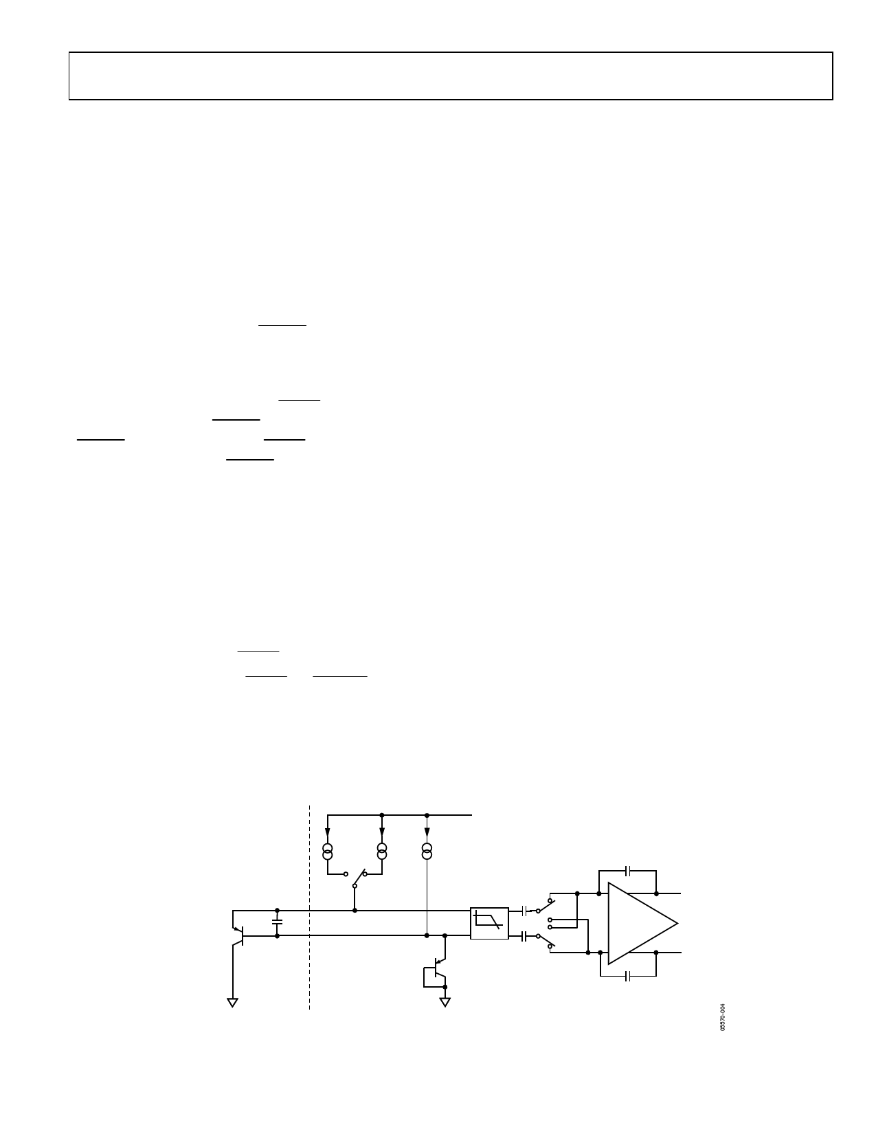
The registers in the ADT7483A are eight bits wide. These
registers are used to store the results of remote and local
temperature measurements, and high and low temperature
limits, and to configure and control the device. A description
of these registers is provided in this section.
Address Pointer Register
The address pointer register does not have, nor does it
require, an address because the first byte of every write
operation is automatically written to this register. The data
in this first byte always contains the address of another
register on the ADT7483A, which is stored in the address
pointer register. It is to this other register address that the
second byte of a write operation is written, or to which a
subsequent read operation is performed.
The power-on default value of the address pointer register
is 0x00, so if a read operation is performed immediately after
power-on without first writing to the address pointer, the
value of the local temperature will be returned, since its
register address is 0x00.
Temperature Value Registers
The ADT7483A has five registers to store the results of
local and remote temperature measurements. These
registers can only be written to by the ADC and can be read
by the user over the SMBus.
The local temperature value register is at Address 0x00
The Remote 1 temperature value high byte register is at
Address 0x01, with the Remote 1 low byte register at
Address 0x10
The Remote 2 temperature value high byte register is at
Address 0x30, with the Remote 2 low byte register at
Address 0x33
The Remote 2 temperature values can be read from
Address 0x01 for the high byte and Address 0x10 for
the low byte if Bit 3 of Configuration Register 1 is set
to 1
To read the Remote 1 temperature values, Bit 3 of
Configuration Register 1 should be set to 0
The power-on default for all five registers is 0x00
Table 9. CONFIGURATION 1 REGISTER (READ ADDRESS = 0x03, WRITE ADDRESS = 0x09)
Bit Mnemonic
Function
7
Mask
Setting this bit to 1 masks all ALERTs on the ALERT pin. Default = 0 = ALERT enabled. This applies only if
Pin 13 is configured as ALERT, otherwise it has no effect.
6 Mon/STBY Setting this bit to 1 places the ADT7483A in standby mode, that is, suspends all temperature measurements
(ADC). The SMBus remains active and values can be written to, and read from, the registers. THERM and
ALERT are also active in standby mode. Changes made to the limit registers in standby mode that affect the
THERM or ALERT outputs will cause these signals to be updated. Default = 0 = temperature monitoring
enabled.
5
AL/TH
This bit selects the function of Pin 13. Default = 0 = ALERT. Setting this bit to 1 configures Pin 13 as the
THERM2 pin.
4
Reserved Reserved for future use.
3 Remote 1/ Setting this bit to 1 enables the user to read the Remote 2 values from the Remote 1 registers.
Remote 2 Default = 0 = Remote 1 temperature values and limits are read from these registers. This bit is not lockable.
2
Temp
Setting this bit to 1 enables the extended temperature measurement range (−50C to +150C).
Range
Default = 0 = 0C to +127C.
1
Mask R1 Setting this bit to 1 masks ALERTs due to the Remote 1 temperature exceeding a programmed limit. Default = 0.
0
Mask R2 Setting this bit to 1 masks ALERTs due to the Remote 2 temperature exceeding a programmed limit. Default = 0.
Table 10. CONFIGURATION 2 REGISTER (ADDRESS = 0x24)
Bit Mnemonic
Function
7
Lock Bit Setting this bit to 1 locks all lockable registers to their current values. This prevents settings being tampered
with until the device is powered down. Default = 0.
<6:0>
Res
Reserved for future use.
http://onsemi.com
9
Share Link: 