ADSP-2184L Ver la hoja de datos (PDF) - Analog Devices
Número de pieza
componentes Descripción
Fabricante
ADSP-2184L Datasheet PDF : 48 Pages
| |||
ADSP-2184L/ADSP-2185L/ADSP-2186L/ADSP-2187L
Table 4. PMOVLAY Bits
Processor
ADSP-2184L
ADSP-2185L
ADSP-2186L
ADSP-2187L
All Processors
All Processors
PMOVLAY
No internal overlay
region
0
No internal overlay
region
0, 4, 5
1
2
Memory
Not Applicable
Internal overlay
Not applicable
Internal overlay
External overlay 1
External overlay 2
Table 5. DMOVLAY Bits
Processor
ADSP-2184L
ADSP-2185L
ADSP-2186L
ADSP-2187L
All Processors
All Processors
DMOVLAY
No internal overlay
region
0
No internal overlay
region
0, 4, 5
1
2
Memory
Not applicable
Internal overlay
Not applicable
Internal overlay
External overlay 1
External overlay 2
I/O Space (Full Memory Mode)
ADSP-218xL series members support an additional external
memory space called I/O space. This space is designed to sup-
port simple connections to peripherals (such as data converters
and external registers) or to bus interface ASIC data registers.
I/O space supports 2048 locations of 16-bit wide data. The lower
eleven bits of the external address bus are used; the upper three
bits are undefined.
Two instructions were added to the core ADSP-2100 family
instruction set to read from and write to I/O memory space. The
I/O space also has four dedicated 3-bit wait state registers,
IOWAIT0–3 as shown in Figure 8, which specify up to seven
wait states to be automatically generated for each of four
regions. The wait states act on address ranges, as shown in
Table 6.
Note: In Full Memory Mode, all 2048 locations of I/O space are
directly addressable. In Host Memory Mode, only address pin
A0 is available; therefore, additional logic is required externally
to achieve complete addressability of the 2048 I/O space
locations.
Table 6. Wait States
Address Range
0x000–0x1FF
0x200–0x3FF
0x400–0x5FF
0x600–0x7FF
Wait State Register
IOWAIT0
IOWAIT1
IOWAIT2
IOWAIT3
A13
Not applicable
Not applicable
Not applicable
Not applicable
0
1
A12 – 0
Not applicable
Not applicable
Not applicable
Not applicable
13 LSBs of address between 0x2000 and 0x3FFF
13 LSBs of address between 0x2000 and 0x3FFF
A13
Not applicable
Not applicable
Not applicable
Not applicable
0
1
A12 – 0
Not applicable
Not applicable
Not applicable
Not applicable
13 LSBs of address between 0x0000 and 0x1FFF
13 LSBs of address between 0x0000 and 0x1FFF
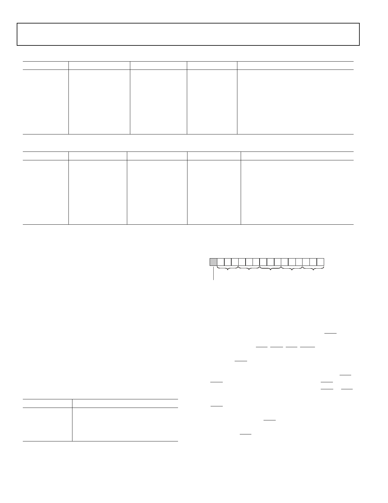
WAIT STATE CONTROL
15 14 13 12 11 10 9 8 7 6 5 4 3 2 1 0
0 1 11 11 11 1 1 1 11 1 1 1
DM(0x3FFE)
DWAIT IOWAIT3 IOWAIT2 IOWAIT1 IOWAIT0
RESERVED
Figure 8. Wait State Control Register
Composite Memory Select
ADSP-218xL series members have a programmable memory
select signal that is useful for generating memory select signals
for memories mapped to more than one space. The CMS signal
is generated to have the same timing as each of the individual
memory select signals (PMS, DMS, BMS, IOMS) but can com-
bine their functionality. Each bit in the CMSSEL register, when
set, causes the CMS signal to be asserted when the selected
memory select is asserted. For example, to use a 32K word
memory to act as both program and data memory, set the PMS
and DMS bits in the CMSSEL register and use the CMS pin to
drive the chip select of the memory, and use either DMS or PMS
as the additional address bit.
The CMS pin functions like the other memory select signals
with the same timing and bus request logic. A 1 in the enable bit
causes the assertion of the CMS signal at the same time as the
selected memory select signal. All enable bits default to 1 at
reset, except the BMS bit.
Rev. C | Page 10 of 48 | January 2008
Share Link: 