ADSP-2184BST-160 Ver la hoja de datos (PDF) - Analog Devices
Número de pieza
componentes Descripción
Fabricante
ADSP-2184BST-160 Datasheet PDF : 31 Pages
| |||
ADSP-2184
When PMOVLAY is set to 1 or 2, external accesses occur at
addresses 0x2000 through 0x3FFF. The external address is
generated as shown in Table II.
Table II.
PMOVLAY Memory A13
A12:0
0
Internal Not Applicable Not Applicable
1
External
Overlay 1 0
13 LSBs of Address
Between 0x2000
and 0x3FFF
2
External
Overlay 2 1
13 LSBs of Address
Between 0x2000
and 0x3FFF
NOTE: Addresses 0x2000 through 0x3FFF should not be accessed when
PMOVLAY = 0.
This organization provides for two external 8K overlay segments
using only the normal 14 address bits, which allows for simple
program overlays using one of the two external segments in
place of the on-chip memory. Care must be taken in using this
overlay space in that the processor core (i.e., the sequencer)
does not take into account the PMOVLAY register value. For
example, if a loop operation is occurring on one of the external
overlays and the program changes to another external overlay or
internal memory, an incorrect loop operation could occur. In
addition, care must be taken in interrupt service routines as the
overlay registers are not automatically saved and restored on the
processor mode stack.
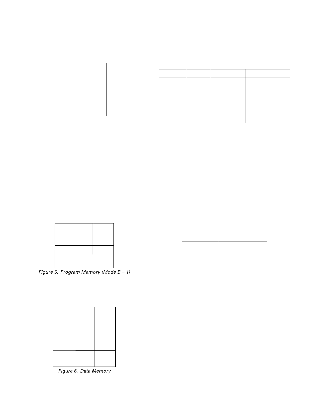
When Mode B = 1, booting is disabled and overlay memory is
disabled the 4K internal PM cannot be accessed with MODE
B = 1. Figure 5 shows the memory map in this configuration.
PROGRAM MEMORY
RESERVED
ADDRESS
0x3FFF
0x2000
0x1FFF
8K EXTERNAL
0x0000
Figure 5. Program Memory (Mode B = 1)
Data Memory
The ADSP-2184 has 4K 16-bit words of internal data memory. In
addition, the ADSP-2184 allows the use of 8K external memory
overlays. Figure 6 shows the organization of the data memory.
DATA MEMORY
ADDRESS
32 MEMORY–
MAPPED REGISTERS
4064
RESERVED
WORDS
INTERNAL
4K WORDS
EXTERNAL 8K
(DMOVLAY = 1, 2)
0x3FFF
0x3FEO
0x3FDF
0x3000
0x2FFF
0x2000
0x1FFF
0x0000
Figure 6. Data Memory
There are 4K words of memory accessible internally when the
DMOVLAY register is set to 0. When DMOVLAY is set to 1 or
2, external accesses occur at addresses 0x0000 through 0x1FFF.
The external address is generated as shown in Table III.
Table III.
DMOVLAY Memory A13
A12:0
0
Internal Not Applicable Not Applicable
1
External
Overlay 1 0
13 LSBs of Address
Between 0x0000
and 0x1FFF
2
External
Overlay 2 1
13 LSBs of Address
Between 0x0000
and 0x1FFF
This organization allows for two external 8K overlays using only
the normal 14 address bits. All internal accesses complete in one
cycle. Accesses to external memory are timed using the wait
states specified by the DWAIT register.
I/O Space (Full Memory Mode)
The ADSP-2184 supports an additional external memory space
called I/O space. This space is designed to support simple con-
nections to peripherals or to bus interface ASIC data registers.
I/O space supports 2048 locations. The lower eleven bits of the
external address bus are used; the upper three bits are unde-
fined. Two instructions were added to the core ADSP-2100
Family instruction set to read from and write to I/O memory
space. The I/O space also has four dedicated three-bit wait state
registers, IOWAIT0-3, that specify up to seven wait states to be
automatically generated for each of four regions. The wait states
act on address ranges as shown in Table IV.
Table IV.
Address Range
0x000–0x1FF
0x200–0x3FF
0x400–0x5FF
0x600–0x7FF
Wait State Register
IOWAIT0
IOWAIT1
IOWAIT2
IOWAIT3
Composite Memory Select (CMS)
The ADSP-2184 has a programmable memory select signal that
is useful for generating memory select signals for memories
mapped to more than one space. The CMS signal is generated
to have the same timing as each of the individual memory select
signals (PMS, DMS, BMS, IOMS), but can combine their
functionality.
Each bit in the CMSSEL register, when set, causes the CMS
signal to be asserted when the selected memory select is as-
serted. For example, to use a 32K word memory to act as both
program and data memory, set the PMS and DMS bits in the
CMSSEL register and use the CMS pin to drive the chip select
of the memory and use either DMS or PMS as the additional
address bit.
The CMS pin functions as the other memory select signals, with
the same timing and bus request logic. A 1 in the enable bit
causes the assertion of the CMS signal at the same time as the
selected memory select signal. All enable bits, except the BMS
bit, default to 1 at reset.
–8–
REV. 0
Share Link: 