ADSP-21161NKCA-100(RevA) Ver la hoja de datos (PDF) - Analog Devices
Número de pieza
componentes Descripción
Fabricante
ADSP-21161NKCA-100 Datasheet PDF : 60 Pages
| |||
ADSP-21161N
synchronous approach, coupled with the core clock frequency,
supports data transfer at a high throughput—up to 400 M bytes/s
for 32-bit transfers and 600 M bytes/s for 48-bit transfers.
The SDRAM interface provides a glueless interface with
standard SDRAMs—16 Mb, 64 Mb, 128 Mb, and 256 Mb—
and includes options to support additional buffers between the
ADSP-21161N and SDRAM. The SDRAM interface is
extremely flexible and provides capability for connecting
SDRAMs to any one of the ADSP-21161N’s four external
memory banks, with up to all four banks mapped to SDRAM.
Systems with several SDRAM devices connected in parallel may
require buffering to meet overall system timing requirements.
The ADSP-21161N supports pipelining of the address and
control signals to enable such buffering between itself and
multiple SDRAM devices.
Target Board JTAG Emulator Connector
Analog Devices DSP Tools product line of JTAG emulators uses
the IEEE 1149.1 JTAG test access port of the ADSP-21161N
processor to monitor and control the target board processor
during emulation. Analog Devices DSP Tools product line of
JTAG emulators provides emulation at full processor speed,
allowing inspection and modification of memory, registers, and
processor stacks. The processor’s JTAG interface ensures that the
emulator will not affect target system loading or timing.
For complete information on SHARC Analog Devices DSP
Tools product line of JTAG emulator operation, see the appro-
priate Emulator Hardware User’s Guide. For detailed infor-
mation on the interfacing of Analog Devices JTAG emulators
with Analog Devices DSP products with JTAG emulation ports,
please refer to Engineer to Engineer Note EE-68: Analog Devices
JTAG Emulation Technical Reference. Both of these documents can
be found on the Analog Devices website:
http://www.analog.com/dsp/tech_docs.html
DMA Controller
The ADSP-21161N’s on-chip DMA controller enables zero-
overhead data transfers without processor intervention. The
DMA controller operates independently and invisibly to the
processor core, allowing DMA operations to occur while the core
is simultaneously executing its program instructions. DMA
transfers can occur between the ADSP-21161N’s internal
memory and external memory, external peripherals, or a host
processor. DMA transfers can also occur between the ADSP-
21161N’s internal memory and its serial ports, link ports, or the
SPI-compatible (Serial Peripheral Interface) port. External bus
packing and unpacking of 32-, 48-, or 64-bit words in internal
memory is performed during DMA transfers from either 8-,
16-, or 32-bit wide external memory. Fourteen channels of DMA
are available on the ADSP-21161N—two are shared between the
SPI interface and the link ports, eight via the serial ports, and
four via the processor’s external port (for host processor, other
ADSP-21161Ns, memory, or I/O transfers). Programs can be
downloaded to the ADSP-21161N using DMA transfers. Asyn-
chronous off-chip peripherals can control two DMA channels
using DMA Request/Grant lines (DMAR2–1, DMAG2–1).
Other DMA features include interrupt generation upon comple-
tion of DMA transfers, and DMA chaining for automatic linked
DMA transfers.
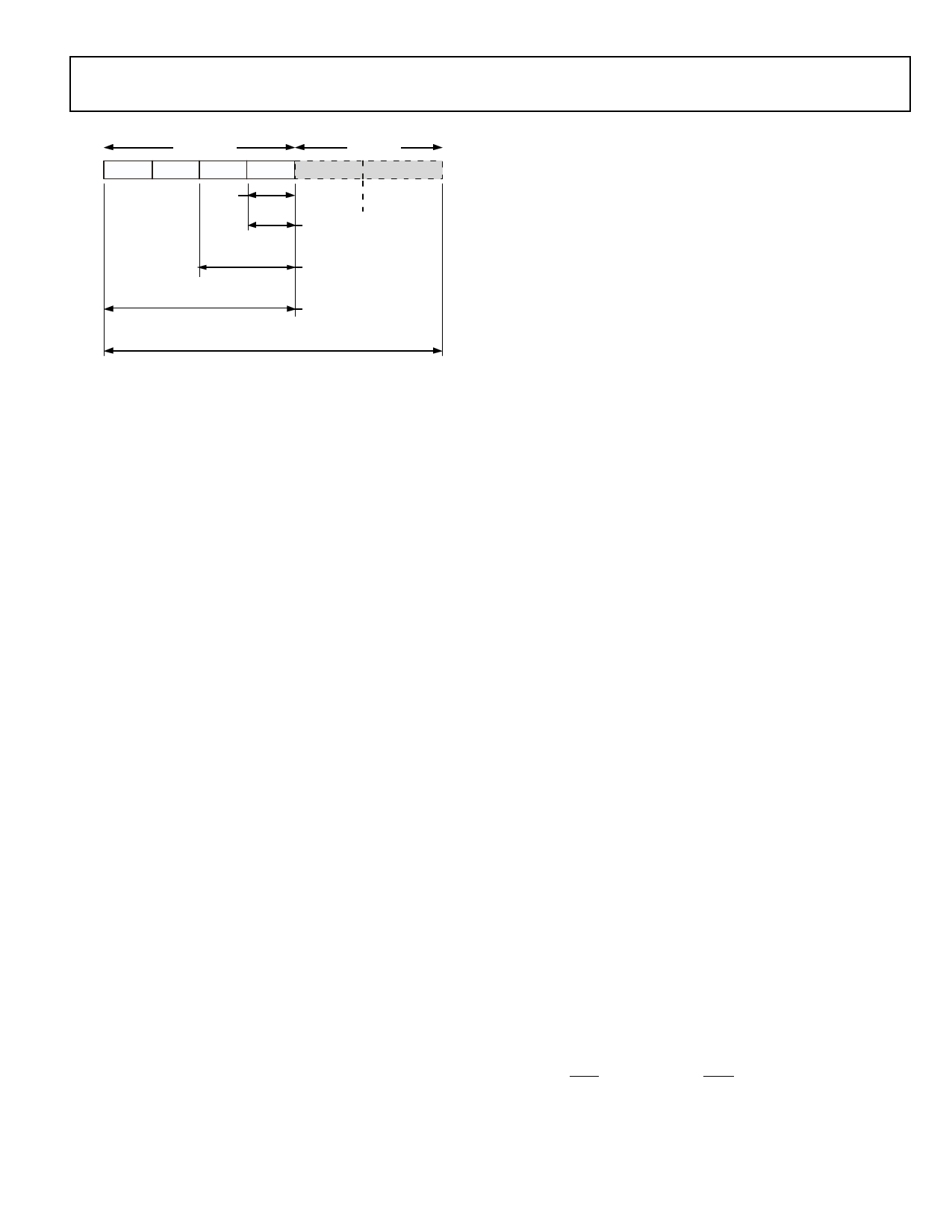
DATA47–16
DATA15–0
47 40 39 32 31 24 23 16 15
87
0
PROM
BO O T
L1DATA7–0 L0DATA7–0
DAT A15-8
DA TA7–0
8-BIT PACKED DMA D ATA
8-BIT PACKED INST RUCT ION
EX ECUTI ON
16-BIT PACKED DMA DATA
16-BIT PACKED INSTRUC-
TION EXECUTION
F LOAT OR FIXED, D31–D0,
32-BIT PA CKED
32-BIT PA CKED INSTRUC-
T ION
48-BIT INSTRUCT ION FETCH
NOTE:
(NO PACKING)
EXTRA DA TA LINES DATA15–0 AR E ONLY ACCESSIBLE IF LINK PORT S
ARE DISABLED. ENAB LE THESE ADDITIONAL DATA L INKS BY SELECT-
ING IPACK1–0 = 01 IN SYSCON.
Figure 3. External Data Alignment Options
Multiprocessing
The ADSP-21161N offers powerful features tailored to
multiprocessing DSP systems. The external port and link ports
provide integrated glueless multiprocessing support.
The external port supports a unified address space (see Figure 2
on Page 6) that enables direct interprocessor accesses of each
ADSP-21161N’s internal memory-mapped (I/O processor) reg-
isters. All other internal memory can be indirectly accessed via
DMA transfers initiated via the programming of the IOP DMA
parameter and control registers. Distributed bus arbitration logic
is included on-chip for simple, glueless connection of systems
containing up to six ADSP-21161Ns and a host processor.
Master processor change over incurs only one cycle of overhead.
Bus arbitration is selectable as either fixed or rotating priority.
Bus lock enables indivisible read-modify-write sequences for
semaphores. A vector interrupt is provided for interprocessor
commands. Maximum throughput for interprocessor data
transfer is 400 M bytes/s over the external port.
Two link ports provide a second method of multiprocessing com-
munications. Each link port can support communications to
another ADSP-21161N. The ADSP-21161N, running at
100 MHz, has a maximum throughput for interprocessor com-
munications over the links of 200 M bytes/s. The link ports and
cluster multiprocessing can be used concurrently or
independently.
Link Ports
The ADSP-21161N features two 8-bit link ports that provide
additional I/O capabilities. With the capability of running at
100 MHz, each link port can support 100 M bytes/s. Link port
I/O is especially useful for point-to-point interprocessor commu-
nication in multiprocessing systems. The link ports can operate
independently and simultaneously, with a maximum data
throughput of 200 M bytes/s. Link port data is packed into
48- or 32-bit words and can be directly read by the core processor
REV. A
–7–
Share Link: 