ADP3171 Ver la hoja de datos (PDF) - Analog Devices
Número de pieza
componentes Descripción
Fabricante
ADP3171 Datasheet PDF : 13 Pages
| |||
ADP3171
5V
5VSB
D1
MBR052LT1
12V
D2
MBR052LT1
5VSB
Q1
2N7000
C1
1F
C2
10F
C3
100pF
+ C5
1000F
+ C6
4.7F
C7
100nF
C8
22F
L1
1.7H
1 GND
DRVH 14
2 PWRGD DRVL 13
3 LRFB1
VCC 12
4 LRDRV1 LRFB2 11
5 FB
LRDRV2 10
6 CS–
COMP 9
7 CS+
CT 8
C9
150pF
R1
220⍀
C3
1nF
R2
220⍀
R3 R4
1k⍀ 249⍀
Q2
FDS6982
C10
100pF
R8
10k⍀
R9
8.25k⍀
5VSB
Q3
IRFU014
C12
1F
+ C13
220F
R6
820F ؋ 4
7.5m⍀ 7.5m⍀ ESR (EACH)
C14 C15 C16 C17
1.5V, 5A
3.3VSB, 1.5A
1.5VSB, 35mA
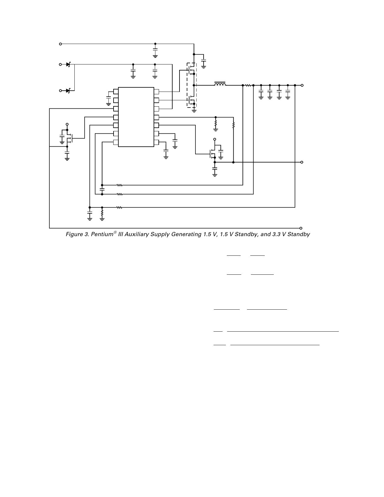
Figure 3. Pentium® III Auxiliary Supply Generating 1.5 V, 1.5 V Standby, and 3.3 V Standby
be disabled in standby mode, but the linear regulators will
begin conducting once VCC rises above about 1 V. During
startup, the linear outputs will track the 3.3 V supply up until
they reach their respective regulation points, regardless of the
state of the 12 V supply. Once the 12 V supply has exceeded
the 5 VSB supply, the controller IC will track the 12 V supply.
Once the 12 V supply has risen above the UVLO value, the
switching regulator will begin its start-up sequence.
tOFF
=
1 –
VOUT
VIN
×
1
fNOM
(1)
tOFF
=
1
–
1.5 V
5V
×
1
200 kHz
= 3.5 µs
The timing capacitor can be calculated from the equation:
APPLICATION INFORMATION
Specifications for a Design Example
The design parameters for a typical auxiliary supply for a Pen-
tium III application (shown in Figure 3) are as follows:
Input Voltage: (VIN) = 5 V
Auxiliary Input: (VCC) = 12 V
Main Output: (VOUT) = 1.5 V @ 5 A
LDO 1 Output: (1.5 VSB) = 1.5 V @ 35 mA
LDO 2 Output: (3.3 VSB) = 3.3 V @ 1.5 A
CT Selection for Operating Frequency
The ADP3171 uses a constant off time architecture, with tOFF
determined by an external timing capacitor CT. Each time the
high side N-channel MOSFET switch turns on, the voltage across
CT is reset to approximately 0 V. During the off time, CT is
charged by a constant current of 150 µA. Once CT reaches 3.0 V,
a new on time cycle is initiated. The value of the off time is
calculated using the continuous-mode operating frequency.
Assuming a nominal operating frequency (fNOM) of 200 kHz at
an output voltage of 1.5 V, the corresponding off time is:
CT
= tOFF × ICT
VT(TH)
= 3.5 µs × 150 µA = 175 pF
3V
(2)
(3) fMIN
=1
tOFF
×
VIN – IO( MAX ) × (RDS (ON )HSF + RSENSE + RL ) – VOUT
VIN – IO( MAX ) × (RDS (ON )HSF + RSENSE + RL – RDS (ON )LSF )
fMIN
=1×
3.5 µs
5V – 5 A × (15 mΩ + 7.5 mΩ + 3 mΩ) – 1.5V = 192 kHz
5V – 5 A × (15 mΩ + 7.5 mΩ + 3 mΩ – 28 mΩ)
The nearest standard value is 150 pF. The converter operates at
the nominal operating frequency only at the above specified VOUT
and at light load. At higher values of VOUT, or under heavy load,
the operating frequency decreases due to the parasitic voltage
drops across the power devices. The actual minimum frequency
at VOUT = 1.5 V is calculated to be 192 kHz (see Equation 3),
where:
RDS(ON)HSF is the resistance of the high side MOSFET
(estimated value: 15 mΩ)
RDS(ON)LSF is the resistance of the low side MOSFET
(estimated value: 28 mΩ)
RSENSE is the resistance of the sense resistor
(estimated value: 7.5 mΩ)
RL is the resistance of the inductor (estimated value: 3 mΩ)
Pentium is a registered trademark of Intel Corporation.
–6–
REV. 0
Share Link: 