ADP3171 Ver la hoja de datos (PDF) - Analog Devices
Número de pieza
componentes Descripción
Fabricante
ADP3171 Datasheet PDF : 13 Pages
| |||
Test Circuits
ADP3171
VCS–
ADP3171
1 GND
DRVH 14
2 PWRGD DRVL 13
3 LRFB1
VCC 12
4 LRDRV1 LRFB2 11
5 FB
LRDRV2 10
6 CS–
COMP 9
7 CS+
CT 8
+
1F
12V
100nF
100⍀
100nF
AD820
1.2V
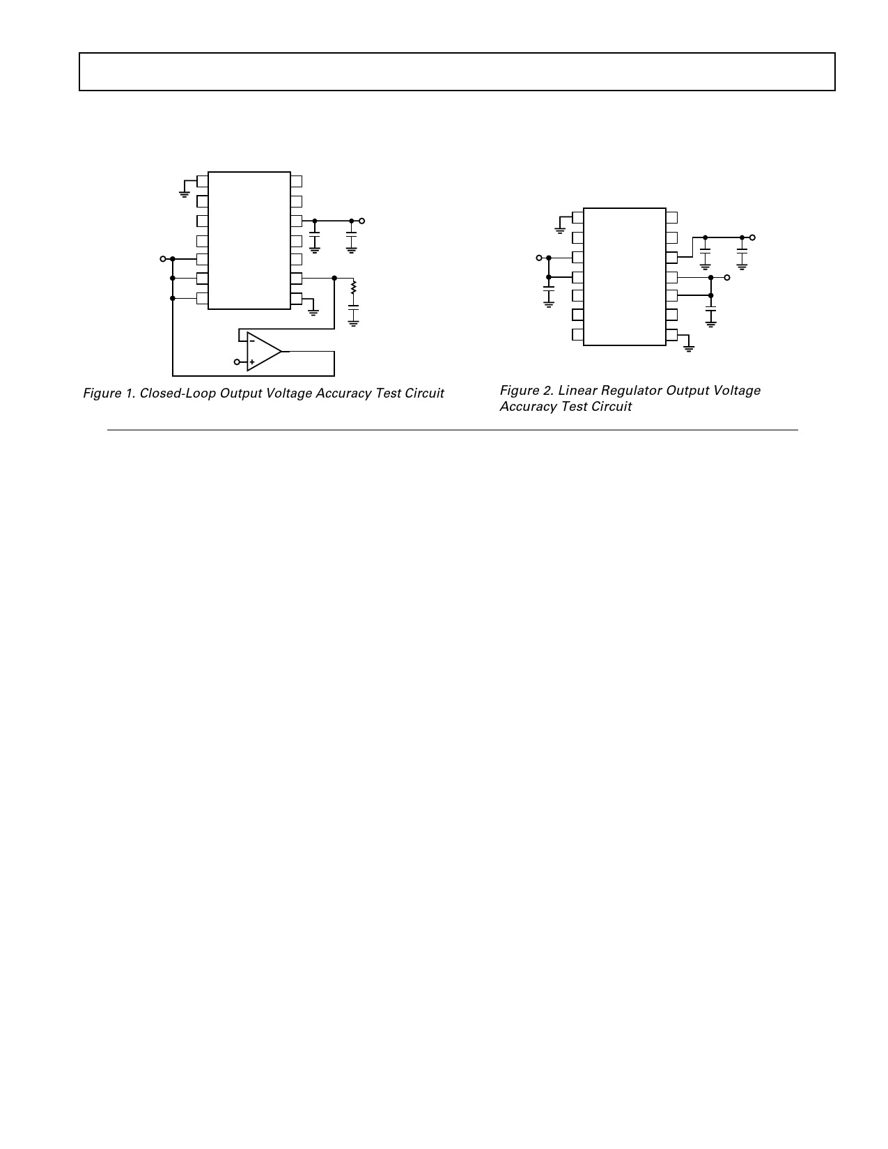
Figure 1. Closed-Loop Output Voltage Accuracy Test Circuit
VLR1
10nF
ADP3171
1 GND
DRVH 14
2 PWRGD DRVL 13
3 LRFB1
VCC 12
4 LRDRV1 LRFB2 11
5 FB
LRDRV2 10
6 CS–
COMP 9
7 CS+
CT 8
+
1F
VCC
100nF
VLR2
10nF
Figure 2. Linear Regulator Output Voltage
Accuracy Test Circuit
THEORY OF OPERATION
The ADP3171 uses a current-mode, constant off time control
technique to switch a pair of external N-channel MOSFETs in a
synchronous buck topology. Constant off time operation offers
several performance advantages, including the fact that no slope
compensation is required for stable operation. A unique feature
of the constant off time control technique is that since the off
time is fixed, the converter’s switching frequency is a function of
the ratio of input voltage to output voltage. The fixed off time is
programmed by the value of an external capacitor connected to
the CT pin. The on time varies in such a way that a regulated
output voltage is maintained as described below in the cycle-by-
cycle operation. Under fixed operating conditions, the on time
does not vary, and it varies only slightly as a function of load.
This means that switching frequency is fairly constant in most
applications.
Cycle-by-Cycle Operation
During normal operation (when the output voltage is regulated),
the voltage error amplifier and the current comparator are the
main control elements. During the on time of the high side
MOSFET, the current comparator monitors the voltage
between the CS+ and CS– pins. When the voltage level between
the two pins reaches the threshold level, the DRVH output is
switched to ground, which turns off the high side MOSFET.
The timing capacitor CT is then charged at a rate determined
by the off time controller. While the timing capacitor is charging,
the DRVL output goes high, turning on the low side MOSFET.
When the voltage level on the timing capacitor has charged to
the upper threshold voltage level, a comparator resets a latch.
The output of the latch forces the low side drive output to go
low and the high side drive output to go high. As a result, the
low side switch is turned off and the high side switch is turned on.
The sequence is then repeated. As the load current increases, the
output voltage starts to decrease. This causes an increase in the
output of the voltage error amplifier, which, in turn, leads to an
increase in the current comparator threshold, thus tracking the
load current. To prevent cross conduction of the external
MOSFETs, feedback is incorporated to sense the state of the driver
output pins. Before the low side drive output can go high, the
high side drive output must be low. Likewise, the high side drive
output is unable to go high while the low side drive output is high.
Output Crowbar
An added feature of using an N-channel MOSFET as the syn-
chronous switch is the ability to crowbar the output with the
same MOSFET. If the output voltage is 20% greater than the
targeted value, the ADP3171 will turn on the lower MOSFET,
which will current-limit the source power supply or blow its
fuse, pull down the output voltage, and thus protect the load
from overvoltage destruction. The crowbar function releases at
approximately 50% of the nominal output voltage. For example,
if the output exceeds 1.44 V, the crowbar will turn on the lower
MOSFET. If the output is then pulled down to less than 0.6 V,
the crowbar will release, allowing the output voltage to recover
to 1.2 V if the fault condition has been removed.
On-Board Linear Regulator Controllers
The ADP3171 includes two linear regulator controllers to
provide a low cost solution for generating additional supply
rails. These regulators are internally set to 1.5 V (LR1) and 1.8 V
(LR2). The output voltage is sensed by the high input imped-
ance LRFB(x) pin and compared to an internal fixed reference.
The LRDRV(x) pin controls the gate of an external N-channel
MOSFET, resulting in a negative feedback loop. The only
additional components required are a capacitor and a resistor
for stability. Higher output voltages can be generated by placing
a resistor divider between the linear regulator output and its
respective LRFB pin. The maximum output load current is
determined by the size and thermal impedance of the external
power MOSFET that is placed in series with the supply and
controlled by the ADP3171.
The linear regulator controllers have been designed so that they
remain active even when the switching controller is in UVLO
mode to ensure that the output voltages of the linear regulators
will track the 3.3 V supply as required by Intel® design specifi-
cations. By diode OR-ing the VCC input of the IC to the 5 VSB
and 12 V supplies as shown in Figure 3, the switching output will
Intel is a registered trademark of Intel Corporation.
REV. 0
–5–
Share Link: 