ADP3171 Ver la hoja de datos (PDF) - Analog Devices
Número de pieza
componentes Descripción
Fabricante
ADP3171 Datasheet PDF : 13 Pages
| |||
ADP3171
PIN FUNCTION DESCRIPTIONS
Pin Mnemonic Function
1 GND
Ground Reference. GND should have a low impedance path to the source of the synchronous MOSFET.
2 PWRGD Power Good Indicator. Open-drain output that signals when the output voltage is in the proper operating range.
3, 11 LRFB1,
LRFB2
Feedback connections for the fixed output voltage linear regulator controllers.
4, 10 LRDRV1, Gate drives for the respective linear regulator N-channel MOSFETs.
LRDRV2
5 FB
Feedback Input. Error amplifier input for remote sensing of the output voltage.
6 CS–
Current Sense Negative Node. Negative input for the current comparator.
7 CS+
Current Sense Positive Node. Positive input for the current comparator. The output current is sensed as a voltage
at this pin with respect to CS–.
8 CT
Timing Capacitor. An external capacitor connected from CT to ground sets the off time of the device.
9 COMP
Error Amplifier Output and Compensation Point. The voltage at this output programs the output current control
level between CS+ and CS–.
12 VCC
Supply Voltage for the ADP3171.
13 DRVL
Low-Side MOSFET Drive. Gate drive for the synchronous rectifier N-channel MOSFET. The voltage at DRVL
swings from GND to VCC.
14 DRVH
High-Side MOSFET Drive. Gate drive for the buck switch N-channel MOSFET. The voltage at DRVH swings
from GND to VCC.
ABSOLUTE MAXIMUM RATINGS*
VCC . . . . . . . . . . . . . . . . . . . . . . . . . . . . . . . –0.3 V to +15 V
DRVH, DRVL, LRDRV1, LRDRV2 . . . . . . –0.3 V to VCC + 0.3 V
All Other Inputs and Outputs . . . . . . . . . . . . –0.3 V to +10 V
Operating Ambient Temperature Range . . . . . . . 0°C to 70°C
Operating Junction Temperature . . . . . . . . . . . . . . . . . . 125°C
Storage Temperature Range . . . . . . . . . . . . –65°C to +150°C
JA . . . . . . . . . . . . . . . . . . . . . . . . . . . . . . . . . . . . . . . 105°C/W
Lead Temperature (Soldering, 10 sec) . . . . . . . . . . . . . 300°C
Vapor Phase (60 sec) . . . . . . . . . . . . . . . . . . . . . . . . . . . 215°C
Infrared (15 sec) . . . . . . . . . . . . . . . . . . . . . . . . . . . . . . 220°C
*This is a stress rating only; operation beyond these limits can cause the device to
be permanently damaged. Unless otherwise specified, all voltages are referenced
to GND.
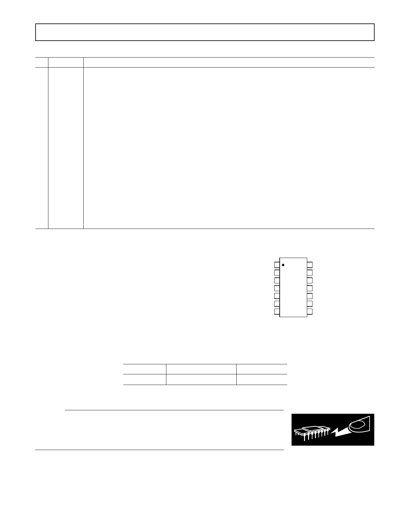
PIN CONFIGURATION
GND 1
14 DRVH
PWRGD 2
13 DRVL
LRFB1 3
12 VCC
ADP3171
LRDRV1 4
11 LRFB2
TOP VIEW
FB 5 (Not to Scale) 10 LRDRV2
CS– 6
9 COMP
CS+ 7
8 CT
Model
ADP3171JR
ORDERING GUIDE
Temperature Range
0ºC to 70ºC
Package Option
SO-14
CAUTION
ESD (electrostatic discharge) sensitive device. Electrostatic charges as high as 4000 V readily
accumulate on the human body and test equipment and can discharge without detection. Although the
ADP3171 features proprietary ESD protection circuitry, permanent damage may occur on devices
subjected to high energy electrostatic discharges. Therefore, proper ESD precautions are recommended
to avoid performance degradation or loss of functionality.
WARNING!
ESD SENSITIVE DEVICE
REV. 0
–3–
Share Link: 