ADN4666ARZ Ver la hoja de datos (PDF) - Analog Devices
Número de pieza
componentes Descripción
Fabricante
ADN4666ARZ Datasheet PDF : 12 Pages
| |||
THEORY OF OPERATION
The ADN4666 is a quad-channel line receiver for low voltage
differential signaling (LVDS). It takes a differential input signal
of 350 mV typical and converts it into a single-ended, 3 V TTL/
CMOS logic signal.
A differential current input signal, received via a transmission
medium such as a twisted pair cable, develops a voltage across
a termination resistor, RT. This resistor is chosen to match the
characteristic impedance of the medium, typically around 100 Ω.
The differential voltage is detected by the receiver and converted
back into a single-ended logic signal.
When the noninverting receiver input, RINx+, is positive with respect
to the inverting input, RINx− (that is, when current flows through
RT from RINx+ to RINx−), ROUTx is high. When the noninverting
receiver input, RINx+, is negative with respect to the inverting
input, RINx− (that is, when current flows through RT from RINx−
to RINx+), ROUTx is low.
Using the ADN4665 as a driver, the received differential current
is between ±2.5 mA and ±4.5 mA (±3.5 mA typical), developing
between ±250 mV and ±450 mV across a 100 Ω termination
resistor. The received voltage is centered around the receiver
offset of 1.2 V. Therefore, the noninverting receiver input is
typically 1.375 V (that is, 1.2 V + [350 mV/2]) and the inverting
receiver input is 1.025 V (that is, 1.2 V − [350 mV/2]) for a
Logic 1. For a Logic 0, the inverting and noninverting input
voltages are reversed. Note that because the differential voltage
reverses polarity, the peak-to-peak voltage swing across RT is
twice the differential voltage.
Current-mode drivers offer considerable advantages over voltage-
mode drivers, such as the RS-422 drivers. The operating current
remains fairly constant with increased switching frequency,
whereas the operating current of voltage-mode drivers increases
exponentially in most cases. This increase is caused by the overlap
as internal gates switch between high and low, causing currents
to flow from VCC to ground. A current-mode device reverses a
constant current between its two outputs, with no significant
overlap currents.
ADN4666
This is similar to emitter-coupled logic (ECL) and positive emitter-
coupled logic (PECL), but without the high quiescent current of
ECL and PECL.
ENABLE INPUTS
The ADN4666 has active high and active low enable inputs that
put all the logic outputs into a high impedance state when disabled,
reducing device current consumption from 10 mA typical to 3 mA
typical. See Table 5 for a truth table of the enable inputs.
Table 5. Enable Inputs Truth Table
Pin Logic Level
EN
EN
RINx+
Low
High
X1
Low
Low
1.025 V
Low
Low
1.375 V
High
Low
1.025 V
High
Low
1.375 V
RINx−
X1
1.375 V
1.025 V
1.375 V
1.025 V
ROUTx
High-Z
0
1
0
1
1 X = don’t care.
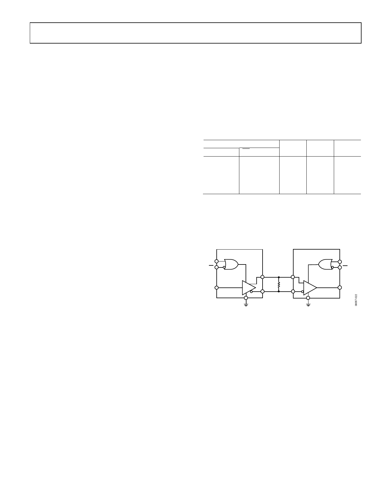
APPLICATIONS INFORMATION
Figure 12 shows a typical application for point-to-point data
transmission using the ADN4665 as the driver and the
ADN4666 as the receiver.
EN
EN
DINx
1/4 ADN4665
GND
1/4 ADN4666
DOUTx+ RINx+
RT
100Ω
DOUTx– RINx–
GND
EN
EN
ROUTx
Figure 12. Typical Application Circuit
Rev. 0 | Page 9 of 12
Share Link: 