ADM1032ARMZ-001 Ver la hoja de datos (PDF) - ON Semiconductor
NГғmero de pieza
componentes DescripciГіn
Fabricante
ADM1032ARMZ-001 Datasheet PDF : 18 Pages
| |||
ADM1032
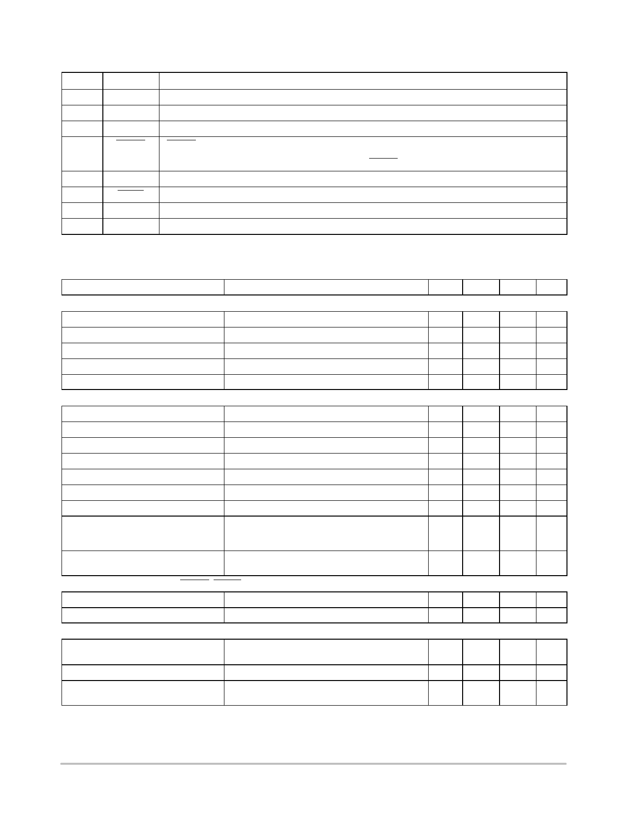
PIN ASSIGNMENT
Pin No.
1
2
Mnemonic
VDD
D+
3
Dв€’
4
THERM
5
GND
6
ALERT
7
SDATA
8
SCLK
Description
Positive Supply, 3.0 V to 5.5 V.
Positive Connection to Remote Temperature Sensor.
Negative Connection to Remote Temperature Sensor.
THERM is an openв€’drain output that can be used to turn a fan on/off or throttle a CPU clock in the event of
an overtemperature condition. Requires pullup to VDD, the same supply as the ADM1032.
Note: Please refer to Power Sequencing Considerations; THERM Pin Pullup on page 15 for more information.
Supply Ground Connection.
Openв€’Drain Logic Output Used as Interrupt or SMBus Alert.
Logic Input/Output, SMBus Serial Data. Openв€’drain output. Requires pullup resistor.
Logic Input, SMBus Serial Clock. Requires pullup resistor.
ELECTRICAL CHARACTERISTICS
Parameter
Power Supply
Supply Voltage, VDD
Average Operating Supply Current, ICC
Undervoltage Lockout Threshold
Powerв€’On Reset Threshold
Temperatureв€’Toв€’Digital Converter
Local Sensor Accuracy
Resolution
Remote Diode Sensor Accuracy
Resolution
Remote Sensor Source Current
Conversion Time
Conditions
0.0625 conversions/sec rate (Note 1)
Standby mode
VDD input, disables ADC, rising edge
0 ≤ TA ≤ 100°C, VCC = 3 V to 3.6 V
60°C ≤ TD ≤ 100°C, VCC = 3 V to 3.6 V
0°C ≤ TD ≤ 120°C
High level (Note 2)
Low level (Note 2)
From stop bit to conversion complete
Both channels: oneв€’shot mode with averaging
switched on
Min
Typ
Max Unit
3.0
3.30
5.5
V
170
215
mA
5.5
10
mA
2.35 2.55
2.8
V
1.0
2.4
V
В±1
В±3
В°C
1.0
В°C
В±1
В°C
В±3
В°C
0.125
В°C
230
mA
13
mA
35.7
142.8 ms
Oneв€’shot mode with averaging off (that is,
5.7
conversion rate = 32 or 64 conversions per second)
22.8 ms
Openв€’Drain Digital Outputs (THERM, ALERT)
Output Low Voltage, VOL
High Level Output Leakage Current, IOH
Serial Bus Timing (Note 2)
IOUT = в€’6.0 mA (Note 2)
VOUT = VDD (Note 2)
Logic Input High Voltage, VIH
SCLK, SDATA
VDD = 3.0 V to 5.5 V
0.4
V
0.1
1.0
mA
2.1
V
Logic Input Low Voltage, VIL
Hysteresis
SCLK, SDATA
VDD = 3.0 V to 5.5 V
0.8
V
500
mV
1. See Table 6 for information on other conversion rates.
2. Guaranteed by design, not production tested.
3. The SMBus timeout is a programmable feature. By default, it is not enabled. Details on how to enable it are available in the Serial Bus
Interface section.
http://onsemi.com
3
Share Link: 