ADL5360 Ver la hoja de datos (PDF) - Analog Devices
Número de pieza
componentes Descripción
Fabricante
ADL5360 Datasheet PDF : 9 Pages
| |||
Preliminary Technical Data
FEATURES
RF Frequency 700MHz to 1000MHz
IF Frequency 50MHZ to 350MHz
Power Conversion Gain of 8.5dB
SSB Noise Figure of 9.5dB
SSB NF with +10dBm blocker of 16.5dB
Input IP3 of 26dBm
Input P1dB of 10 dBm
Typical LO Drive of 0 dBm
Single-ended, 50Ω RF and LO Input Ports
High Isolation SPDT LO Input Switch
Single Supply Operation: 3.3 to 5 V
Exposed Paddle 6 x 6 mm, 36 Lead LFCSP Package
APPLICATIONS
Cellular Base Station Receivers
Main and Diversity Receiver Designs
Radio Link Downconverters
GENERAL DESCRIPTION
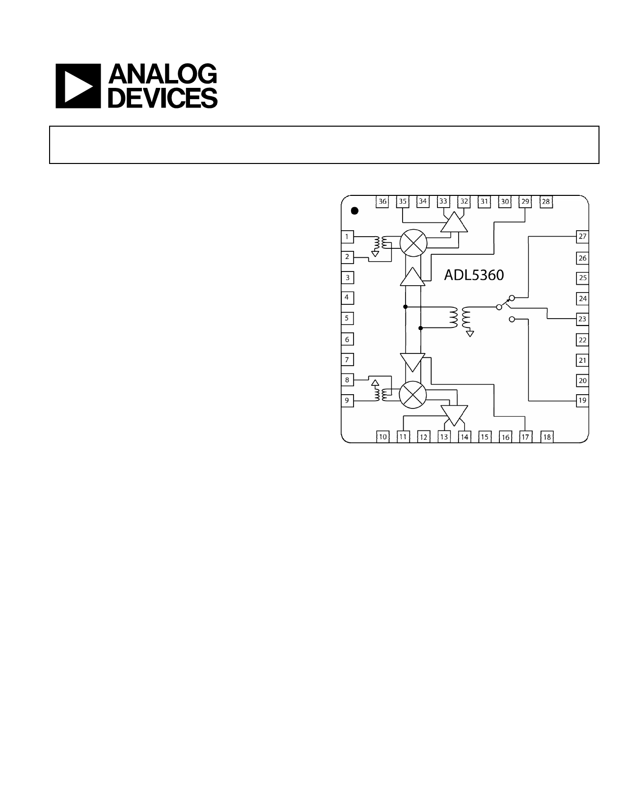
The ADL5360 utilizes two highly linear doubly balanced passive
mixer cores along with integrated RF and LO balancing
circuitry to enable single-ended operation. The ADL5360
incorporates two RF baluns allowing for optimal main and
diversity mixer performance over a 700 to 1000 MHz RF input
frequency range using low-side LO injection. The balanced
passive mixer arrangement provides good LO to RF leakage,
typically better than -25dBm, and excellent intermodulation
performance. The balanced mixer cores also provide extremely
high input linearity allowing the device to be used in
demanding cellular applications where in-band blocking signals
may otherwise result in the degradation of dynamic
performance. High linearity IF buffer amps follow the passive
mixer cores, to yield a typical power conversion gain of 9.5dB.
(For a higher IIP3 version of the dual mixer without the IF
amplifiers, please contact the factory).
The ADL5360 provides two switched LO paths that can be
utilized in TDD applications where it is desirable to rapidly
alternate between two local oscillators. LO current can be
externally set using a resistor to minimize DC current
REV. PrA
Information furnished by Analog Devices is believed to be accurate and reliable.
However, no responsibility is assumed by Analog Devices for its use, nor for any
infringements of patents or other rights of third parties that may result from its use.
Specifications subject to change without notice. No license is granted by implication
or otherwise under any patent or patent rights of Analog Devices. Trademarks and
registered trademarks are the property of their respective companies.
Dual 900MHz Balanced Mixer
with Low Side LO Buffer,
IF Amp, and RF Balun
ADL5360
Figure 1. Functional Block Diagram
commensurate with the desired level of performance. An
additional 3V logic pin is provided to power down (<100uA)
the circuit when desired.
For low voltage applications, the ADL5360 is capable of
operation at voltages down to 3V with substantially reduced DC
current.
The ADL5360 is fabricated using a BiCMOS high performance
IC process. The device is available in a 6mm x 6mm 36-lead
LFCSP package and operates over a −40°C to +85°C
temperature range. An evaluation board is also available.
One Technology Way, P.O. Box 9106, Norwood, MA 02062-9106, U.S.A.
Tel: 781.329.4700
www.analog.com
Fax: 781.326.8703 © 2008 Analog Devices, Inc. All rights reserved.
Share Link: 