ADL5357 Ver la hoja de datos (PDF) - Analog Devices
Número de pieza
componentes Descripción
Fabricante
ADL5357 Datasheet PDF : 24 Pages
| |||
ADL5357
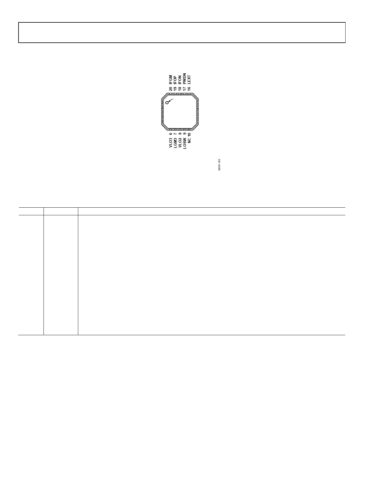
PIN CONFIGURATION AND FUNCTION DESCRIPTIONS
VPIF 1
RFIN 2
RFCT 3
COMM 4
COMM 5
PIN 1
INDICATOR
ADL5357
TOP VIEW
(Not to Scale)
15 LOI2
14 VPSW
13 VGS1
12 VGS0
11 LOI1
NOTES
1. NC = NO CONNECT.
2. EXPOSED PAD. MUST BE SOLDERED
TO GROUND.
Figure 2. Pin Configuration
Table 6. Pin Function Descriptions
Pin No. Mnemonic Description
1
VPIF
Positive Supply Voltage for IF Amplifier.
2
RFIN
RF Input. Must be ac-coupled.
3
RFCT
RF Balun Center Tap (AC Ground).
4, 5
COMM
Device Common (DC Ground).
6, 8
VLO3, VLO2 Positive Supply Voltages for LO Amplifier.
7
LGM3
LO Amplifier Bias Control.
9
LOSW
LO Switch. LOI1 selected for 0 V, and LOI2 selected for 3 V.
10
NC
No Connect.
11, 15 LOI1, LOI2 LO Inputs. Must be ac-coupled.
12, 13 VGS0, VGS1 Mixer Gate Bias Controls. 3 V logic. Ground these pins for nominal setting.
14
VPSW
Positive Supply Voltage for LO Switch.
16
LEXT
IF Return. This pin must be grounded.
17
PWDN
Power Down. Connect this pin to ground for normal operation and connect this pin to 3.0 V for disable mode.
18, 19 IFON, IFOP Differential IF Outputs (Open Collectors). Each requires an external dc bias.
20
IFGM
IF Amplifier Bias Control.
EPAD (EP) Exposed pad. Must be soldered to ground.
Rev. 0 | Page 6 of 24
Share Link: 