ADG508A Ver la hoja de datos (PDF) - Analog Devices
Número de pieza
componentes Descripción
Fabricante
ADG508A Datasheet PDF : 16 Pages
| |||
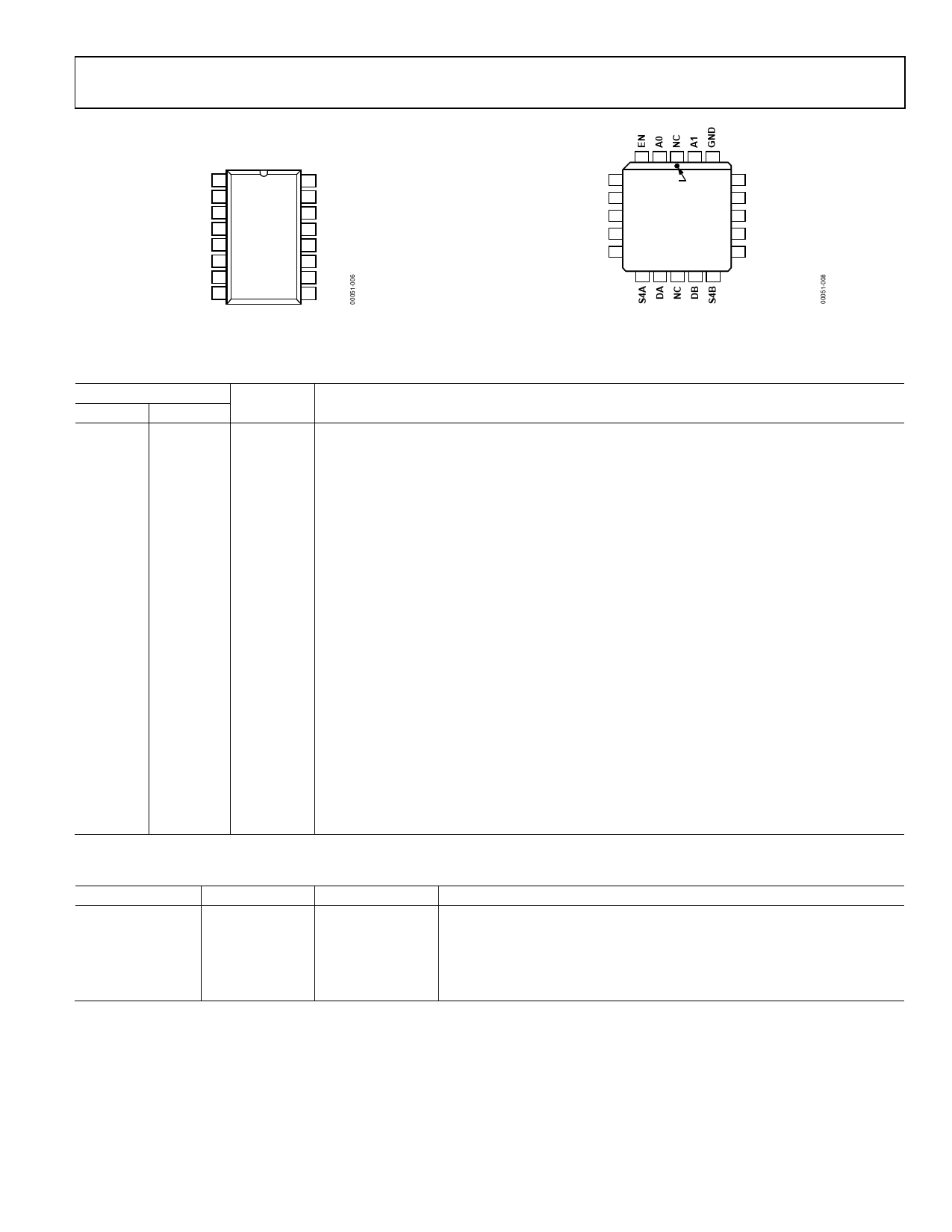
ADG508A/ADG509A
A0 1
EN 2
VSS 3
S1A 4
S2A 5
S3A 6
S4A 7
DA 8
16 A1
15 GND
ADG509A
TOP VIEW
(Not to Scale)
14 VDD
13 S1B
12 S2B
11 S3B
10 S4B
9 DB
Figure 6. ADG509A DIP, SOIC
VSS 4
S1A 5
NC 6
S2A 7
S3A 8
3 2 1 20 19
PIN 1
IDENTIFIER
ADG509A
TOP VIEW
(Not to Scale)
18 VDD
17 S1B
16 NC
15 S2B
14 S3B
9 10 11 12 13 NC = NO CONNECT
Figure 7. ADG509A PLCC
Table 6. ADG509A Pin Function Description
Pin Number
DIP/SOIC PLCC/LCC Mnemonic Description
1
2
A0
Logic Control Input.
2
3
EN
Active High Digital Input. When low, the device is disabled and all switches are off.
When high, Ax logic inputs determine on switches.
3
4
VSS
Most Negative Power Supply Potential in Dual Supplies. In single-supply applications,
it can be connected to ground.
4
5
S1A
Source Terminal 1A. Can be an input or an output.
5
7
S2A
Source Terminal 2A. Can be an input or an output.
6
8
S3A
Source Terminal 3A. Can be an input or an output.
7
9
S4A
Source Terminal 4A. Can be an input or an output.
8
10
DA
Drain Terminal A. Can be an input or an output.
9
12
DB
Drain Terminal B. Can be an input or an output.
10
13
S4B
Source Terminal 4B. Can be an input or an output.
11
14
S3B
Source Terminal 3B. Can be an input or an output.
12
15
S2B
Source Terminal 2B. Can be an input or an output.
13
17
S1B
Source Terminal 1B. Can be an input or an output.
14
18
VDD
Most Positive Power Supply Potential.
15
19
GND
Ground (0 V) Reference.
16
20
A1
Logic Control Input.
N/A
1
NC
No Connect.
N/A
6
NC
No Connect.
N/A
11
NC
No Connect.
N/A
16
NC
No Connect.
Table 7. ADG509A Truth Table
A1
A0
EN
X1
X1
0
X
0
0
1
0
1
1
1
0
1
1
1
1
1 X = don’t care.
On Switch Pair
None
1
2
3
4
Rev. D | Page 9 of 16
Share Link: 