ADE7762 Ver la hoja de datos (PDF) - Analog Devices
Número de pieza
componentes Descripción
Fabricante
ADE7762 Datasheet PDF : 28 Pages
| |||
Preliminary Technical Data
ADE7762
TIMING CHARACTERISTICS
VDD = 5 V ± 5%, AGND = DGND = 0 V, on-chip reference, CLKIN = 10 MHz, TMIN to TMAX = −40°C to +85°C, unless otherwise noted.
Table 2.
Parameter 1 , 2
t1 3
t2
Conditions
F1 and F2 pulse width (logic high)
Output pulse period (see the Transfer Function section)
Specification Unit
120
ms
See Figure 2 sec
t3
Time between F1 falling edge and F2 falling edge
1/2 t2
sec
t43, 4
CF pulse width (logic high)
90
ms
t5 5
CF pulse period (see the Transfer Function section)
See Table 7 sec
t6
Minimum time between F1 and F2 pulse
4/CLKIN
sec
t7
LED_CTRL pulse width
28.8
μs
t8
LED_CTRL period
57.5
μs
t9
LED pulse width
7.2
μs
1 Sample tested during initial release and after any redesign or process changes that might affect this parameter.
2 See Figure 2.
3 The pulse widths of F1, F2, and CF are not fixed for higher output frequencies (see the Frequency Outputs section).
4 CF is not synchronous to F1 or F2 frequency outputs.
5 The CF pulse is always 1 μs in the high frequency mode (see the Frequency Outputs section).
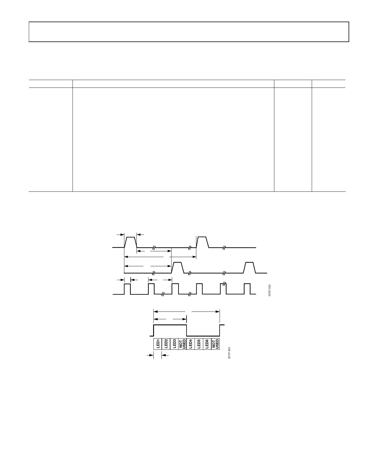
t1
F1
t6
t2
F2
t3
t4
t5
CF
Figure 2. Timing Diagram for Frequency Outputs
t8
t7
t9
Figure 3: Timing Diagram for LED Drivers
Rev. PrB | Page 5 of 28
Share Link: 