ADE7762(Rev0) Ver la hoja de datos (PDF) - Analog Devices
Número de pieza
componentes Descripción
Fabricante
ADE7762 Datasheet PDF : 28 Pages
| |||
ADE7762
Parameter
POWER SUPPLY
VDD
IDD
Conditions
For specified performance
5 V ± 5%
1 See the Terminology section for explanation of specifications.
2 See the plots in the Typical Performance Characteristics section.
3 Sample tested during initial release and after any redesign or process changes that might affect this parameter.
Min Typ Max Unit
4.75
8.5
5.25 V
10 mA
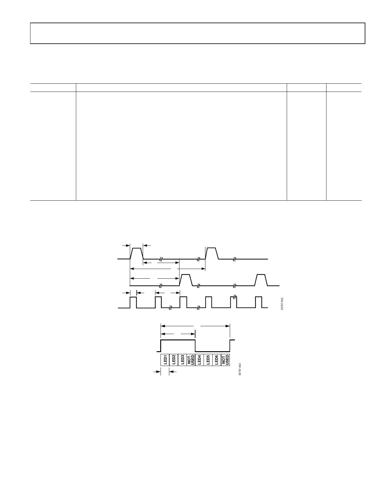
TIMING CHARACTERISTICS
VDD = 5 V ± 5%, AGND = DGND = 0 V, on-chip reference, CLKIN = 10 MHz, TMIN to TMAX = −40°C to +85°C, unless otherwise noted.
Table 2.
Parameter1,2
t1 3
t2
t3
t43, 4
t55
t6
t7
t8
t9
Conditions
F1 and F2 pulse width (logic high)
Output pulse period (see the Transfer Function section)
Time between F1 rising edge and F2 rising edge
CF pulse width (logic high)
CF pulse period (see the Transfer Function section)
Minimum time between F1 and F2 pulse
LED_CTRL pulse width
LED_CTRL period
LED pulse width
Value
Unit
120
ms
See Figure 2
sec
½ t2
sec
90
ms
See Table 7
sec
4/CLKIN
sec
28.8
μs
57.5
μs
7.2
μs
1 Sample tested during initial release and after any redesign or process changes that might affect this parameter.
2 See Figure 2.
3 The pulse widths of F1, F2, and CF are not fixed for higher output frequencies (see the Frequency Outputs section).
4 CF is not synchronous to F1 or F2 frequency outputs.
5 The CF pulse is always 1 μs in the high frequency mode (see the Frequency Outputs section).
t1
F1
t6
t2
F2
t3
t4
t5
CF
Figure 2. Timing Diagram for Frequency Outputs
t8
t7
t9
Figure 3. Timing Diagram for LED Drivers
Rev. 0 | Page 5 of 28
Share Link: 