ADE7760 Ver la hoja de datos (PDF) - Analog Devices
Número de pieza
componentes Descripción
Fabricante
ADE7760 Datasheet PDF : 24 Pages
| |||
ADE7760
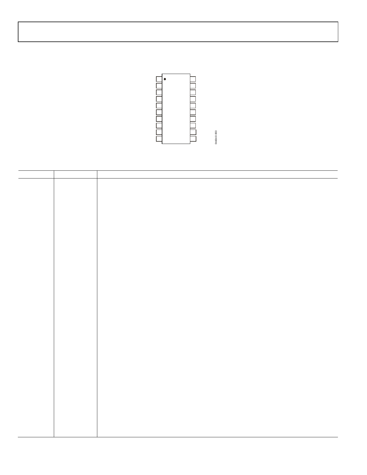
PIN CONFIGURATION AND FUNCTION DESCRIPTIONS
VDD 1
20 F1
V1A 2
19 F2
V1B 3
18 CF
V1N 4
17 DGND
V2N 5
ADE7760
TOP VIEW
16 REVP
V2P 6 (Not to Scale) 15 FAULT
NC 7
14 RCLKIN
AGND 8
13 INT
REFIN/OUT 9
12 S0
SCF 10
11 S1
NC = NO CONNECT
Figure 3. Pin Configuration (SSOP)
Table 4. Pin Function Descriptions
Pin No.
Mnemonic
Description
1
VDD
Power Supply. This pin provides the supply voltage for the digital circuitry in the ADE7760. The supply
voltage should be maintained at 5 V ± 5% for specified operation. This pin should be decoupled with a
10 µF capacitor in parallel with a ceramic 100 nF capacitor.
2, 3
V1A, V1B
Analog Inputs for Channel 1 (Current Channel). These inputs are fully differential voltage inputs with
maximum differential input signal levels of ±660 mV with respect to V1N for specified operation. The
maximum signal level at these pins is ±1 V with respect to AGND. Both inputs have internal ESD
protection circuitry, and an overvoltage of ±6 V can also be sustained on these inputs without risk of
permanent damage.
4
V1N
Negative Input Pin for Differential Voltage Inputs V1A and V1B. The maximum signal level at this pin is
±1 V with respect to AGND. The input has internal ESD protection circuitry, and an overvoltage of ±6 V
can also be sustained on these inputs without risk of permanent damage. The input should be directly
connected to the burden resistor and held at a fixed potential, that is, AGND. See the Analog Inputs
section.
5
V2N
Negative Input Pin for Differential Voltage Input V2P. The maximum signal level at this pin is ±1 V with
respect to AGND. The input has internal ESD protection circuitry, and an overvoltage of ±6 V can also be
sustained on these inputs without risk of permanent damage. The input should be held at a fixed
potential, that is, AGND. See the Analog Inputs section.
6
V2P
Analog Inputs for Channel 2 (Voltage Channel). This input is fully differential voltage input with
maximum differential input signal levels of ±660 mV with respect to V2N for specified operation. The
maximum signal level at these pins is ±1 V with respect to AGND. This input has internal ESD protection
circuitry, and an overvoltage of ±6 V can also be sustained on these inputs without risk of permanent
damage.
7
NC
Not Connected. Nothing should be connected to this pin.
8
AGND
This pin provides the ground reference for the analog circuitry in the ADE7760, that is, ADCs and
reference. This pin should be tied to the analog ground plane of the PCB. The analog ground plane is the
ground reference for all analog circuitry such as antialiasing filters, and current and voltage transducers.
For good noise suppression, the analog ground plane should be connected only to the digital ground
plane at the DGND pin.
9
REFIN/OUT
This pin provides access to the on-chip voltage reference. The on-chip reference has a nominal value of
2.5 V ± 8% and a typical temperature coefficient of 30 ppm/°C. An external reference source can also be
connected at this pin. In either case, this pin should be decoupled to AGND with a 1 μF ceramic
capacitor and 100 nF ceramic capacitor.
10
SCF
Select Calibration Frequency. This logic input is used to select the frequency on the calibration output
CF. Table 6 shows how the calibration frequencies are selected.
11, 12
S1, S0
These logic inputs are used to select one of four possible frequencies for the digital-to-frequency
conversion. This offers the designer greater flexibility when designing the energy meter. See the
Selecting a Frequency for an Energy Meter Application section.
13
INT
This pin is internally used and should be connected to DGND.
14
RCLKIN
To enable the internal oscillator as a clock source on the chip, a precise low temperature drift resistor at
nominal value of 6.2 kΩ must be connected from this pin to DGND.
Rev. 0 | Page 8 of 24
Share Link: 