ADE7760 Ver la hoja de datos (PDF) - Analog Devices
Número de pieza
componentes Descripción
Fabricante
ADE7760 Datasheet PDF : 24 Pages
| |||
OPERATION
POWER SUPPLY MONITOR
The ADE7760 contains an on-chip power supply monitor. The
power supply (VDD) is continuously monitored by the ADE7760.
If the supply is less than 4 V ± 5%, the ADE7760 goes into an
inactive state, that is, no energy is accumulated and the CF, F1,
and F2 outputs is disabled. This is useful to ensure correct
device operation at power-up and during power-down. The
power supply monitor has built-in hysteresis and filtering. This
gives a high degree of immunity to false triggering due to noisy
supplies.
The power supply and decoupling for the part should be such
that the ripple at VDD does not exceed 5 V ± 5% as specified for
normal operation.
VDD
5V
4V
0V
ADE7760
REVP - FAULT - CF - INACTIVE
F1 - F2 OUTPUTS
TIME
ACTIVE
INACTIVE
Figure 8. On-Chip Power Supply Monitoring
ANALOG INPUTS
Channel V1 (Current Channel)
The voltage outputs from the current transducers are connected
to the ADE7760 here. Channel V1 has two voltage inputs, V1A
and V1B. These inputs are fully differential with respect to V1N.
However, at any one time, only one is selected to perform the
power calculation (see the Fault Detection section).
The maximum peak differential signal on V1A–V1N and V1B–V1N
is ±660 mV. Figure 9 shows the maximum signal levels on V1A,
V1B, and V1N. The differential voltage signal on the inputs must
be referenced to a common mode such as AGND.
V1A, V1B
+660mV + VCM
VCM
–660mV + VCM
DIFFERENTIAL INPUT A
±660mV MAX PEAK
COMMON MODE
±100mV MAX
VCM
AGND
DIFFERENTIAL INPUT B
±660mV MAX PEAK
V1A
V1
V1N
V1
V1B
Figure 9. Maximum Signal Levels, Channel 1
ADE7760
Channel V2 (Voltage Channel)
The output of the line voltage transducer is connected to the
ADE7760 at this analog input. Channel V2 is a single-ended
voltage input. The maximum peak differential signal on
Channel 2 is ±660 mV with respect to V2N. Figure 10 shows the
maximum signal levels that can be connected to Channel 2.
V2
+660mV + VCM
VCM
–660mV + VCM
DIFFERENTIAL INPUT
±660mV MAX PEAK
COMMON MODE
±100mV MAX
V2P
V2
V2N
VCM
Figure 10. Maximum Signal Levels, Channel 2
The differential voltage V2P–V2N must be referenced to a
common mode (usually AGND). The analog inputs of the
ADE7760 can be driven with common-mode voltages of up to
100 mV with respect to AGND. However, the best results are
achieved using a common mode equal to AGND.
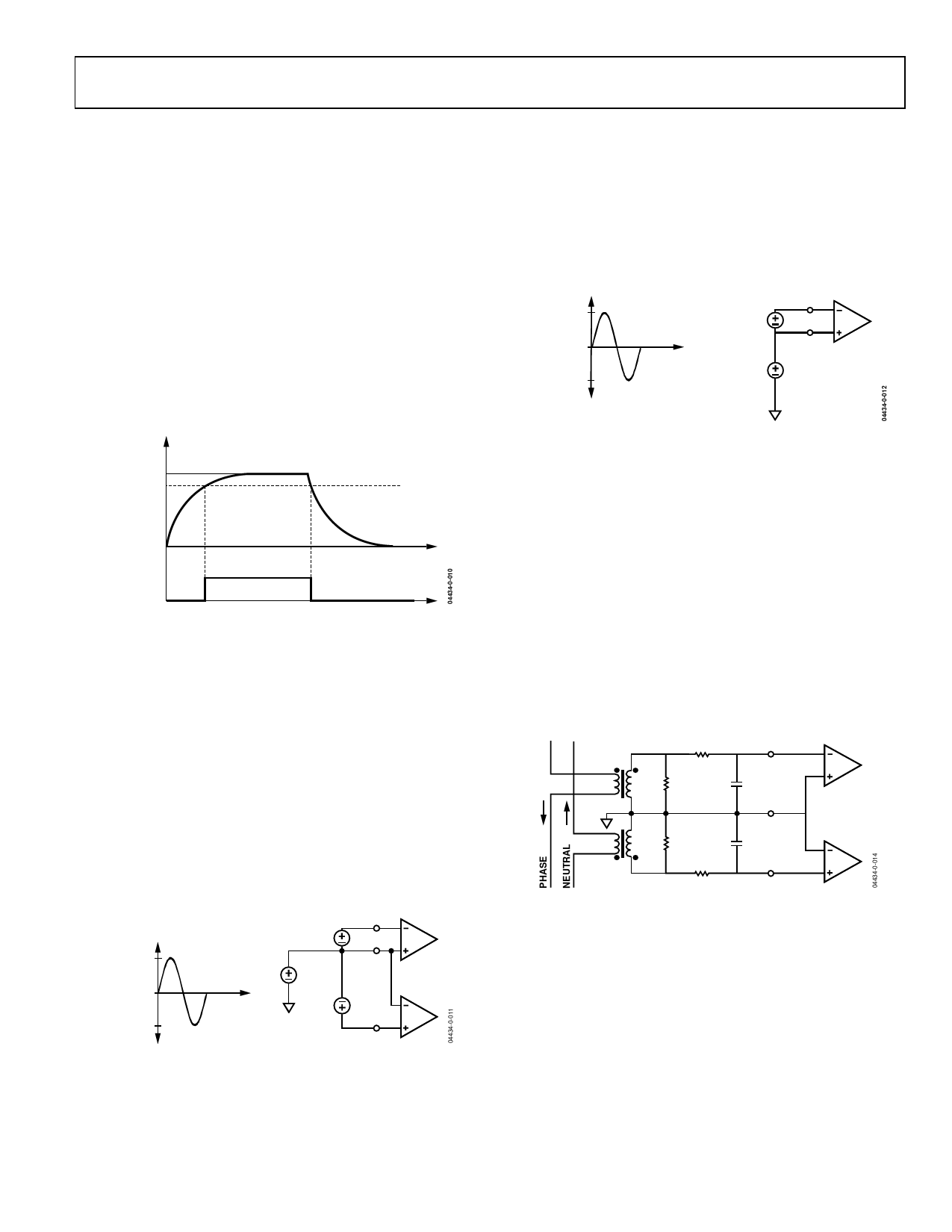
Typical Connection Diagrams
Figure 11 shows a typical connection diagram for Channel V1.
The analog inputs are being used to monitor both the phase and
neutral currents. Because of the large potential difference
between the phase and neutral, two current transformers (CTs)
must be used to provide the isolation. Note that both CTs are
referenced to AGND (analog ground); the common-mode
voltage is, therefore, 0 V. The CT turns ratio and burden resistor
(RB) are selected to give a peak differential voltage of ±660 mV.
RF
V1A
CT
RB
IP IN AGND
RB
CF
V1N
CF
CT
RF
V1B
Figure 11. Typical Connection for Channel 1
Figure 12 shows two typical connections for Channel V2. The
first option uses a potential transformer (PT) to provide
complete isolation from the main voltage. In the second option,
the ADE7760 is biased around the neutral wire, and a resistor
divider is used to provide a voltage signal that is proportional to
the line voltage. Adjusting the ratio of RA and RB + VR is a
convenient way of carrying out a gain calibration on the meter.
Rev. 0 | Page 11 of 24
Share Link: 