ADE7754 Ver la hoja de datos (PDF) - Analog Devices
Número de pieza
componentes Descripción
Fabricante
ADE7754 Datasheet PDF : 44 Pages
| |||
ADE7754
TERMINOLOGY
Measurement Error
The error associated with the energy measurement made by the
ADE7754 is defined by the formula
Percentage Error =
Energy
Registered by ADE7754
True Energy
−
True
Energy
×
100%
Phase Error Between Channels
The HPF (high-pass filter) in the current channel has a phase
lead response. To offset this phase response and equalize the
phase response between channels, a phase correction network is
placed in the current channel. The phase correction network
ensures a phase match between the current channels and voltage
channels to within ± 0.1° over a range of 45 Hz to 65 Hz and
± 0.2° over a range of 40 Hz to 1 kHz. This phase mismatch
between the voltage and the current channels can be reduced
further with the phase calibration register in each phase.
Power Supply Rejection
This quantifies the ADE7754 measurement error as a percentage
of reading when power supplies are varied. For the ac PSR mea-
surement, a reading at nominal supplies (5 V) is taken. A second
reading is obtained using the same input signal levels when an ac
(175 mV rms/100 Hz) signal is introduced onto the supplies. Any
error introduced by this ac signal is expressed as a percentage of
reading. See the Measurement Error definition above.
For the dc PSR measurement, a reading at nominal supplies
(5 V) is taken. A second reading is obtained using the same
input signal levels when the power supplies are varied ± 5%. Any
error introduced is again expressed as a percentage of reading.
ADC Offset Error
This refers to the dc offset associated with the analog inputs to
the ADCs. It means that with the analog inputs connected to
AGND, the ADCs still see a dc analog input signal. The magni-
tude of the offset depends on the gain and input range selection
(see the TPCs). However, when HPFs are switched on, the
offset is removed from the current channels and the power
calculation is unaffected by this offset.
Gain Error
The gain error in the ADE7754 ADCs is defined as the differ-
ence between the measured ADC output code (minus the
offset) and the ideal output code. See the Current Channel
ADC and the Voltage Channel ADC sections. The difference is
expressed as a percentage of the ideal code.
Gain Error Match
Gain error match is defined as the gain error (minus the offset)
obtained when switching between a gain of 1, 2, or 4. It is
expressed as a percentage of the output ADC code obtained
under a gain of 1.
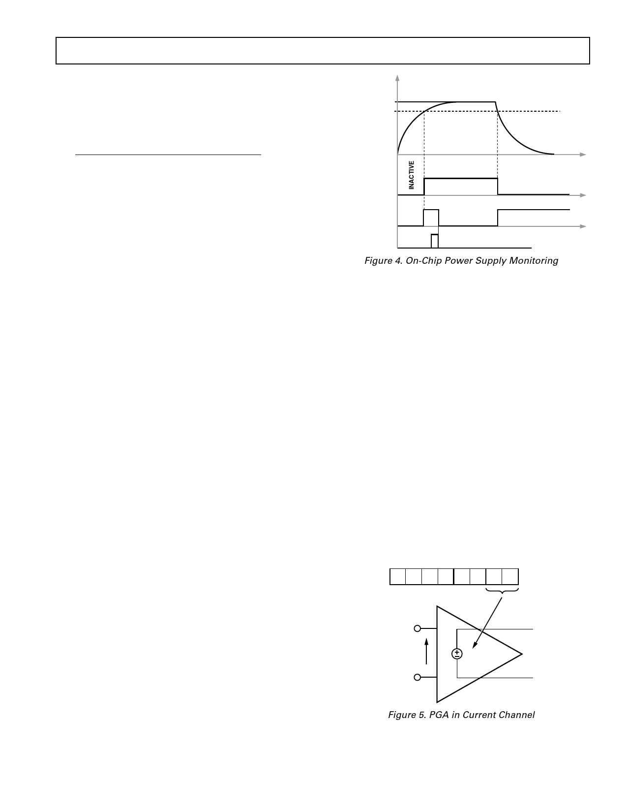
POWER SUPPLY MONITOR
The ADE7754 contains an on-chip power supply monitor. The
analog supply (AVDD) is continuously monitored by the ADE7754.
If the supply is less than 4 V ± 5%, the ADE7754 goes into an
inactive state (i.e., no energy is accumulated when the supply
voltage is below 4 V). This is useful to ensure correct device
operation at power-up and during power-down. The power sup-
ply monitor has built-in hysteresis and filtering, providing a high
degree of immunity to false triggering due to noisy supplies.
AVDD
5V
4V
0V
TIME
POWER-ON
ACTIVE
INACTIVE
RESET FLAG IN
THE INTERRUPT
STATUS REGISTER
READ RSTATUS
REGISTER
Figure 4. On-Chip Power Supply Monitoring
The RESET bit in the interrupt status register is set to Logic 1
when AVDD drops below 4 V ± 5%. The RESET flag is always
masked by the interrupt enable register and cannot cause the
IRQ pin to go low. The power supply and decoupling for the
part should ensure that the ripple at AVDD does not exceed 5 V
± 5% as specified for normal operation.
ANALOG INPUTS
The ADE7754 has six analog inputs, divisible into two chan-
nels: current and voltage. The current channel consists of three
pairs of fully differential voltage inputs: IAP, IAN; IBP, IBN; and
ICP, ICN. The fully differential voltage input pairs have a maxi-
mum differential voltage of ± 0.5 V. The voltage channel has
three single-ended voltage inputs: VAP, VBP, and VCP. These
single-ended voltage inputs have a maximum input voltage of
± 0.5 V with respect to VN. Both the current channel and the
voltage channel have a PGA (programmable gain amplifier) with
possible gain selections of 1, 2, or 4. The same gain is applied to
all the inputs of each channel.
The gain selections are made by writing to the gain register. Bits 0
and 1 select the gain for the PGA in the fully differential current
channel. The gain selection for the PGA in the single-ended volt-
age channel is made via Bits 5 and 6. Figure 5 shows how a gain
selection for the current channel is made using the gain register.
GAIN[7:0]
IAP, IBP, ICP
GAIN (k)
SELECTION
VIN
k ؋ VIN
IAN, IBN, ICN
Figure 5. PGA in Current Channel
REV. 0
–9–
Share Link: 