ADE7754 Ver la hoja de datos (PDF) - Analog Devices
Número de pieza
componentes Descripción
Fabricante
ADE7754 Datasheet PDF : 44 Pages
| |||
ADE7754
TIMING CHARACTERISTICS1, 2 (AVDD = DVDD = 5 V ؎ 5%, AGND = DGND = 0 V, On-Chip Reference, CLKIN = 10 MHz XTAL,
TMIN to TMAX = –40؇C to +85؇C, unless otherwise noted.)
Parameter
Spec
Unit
Test Conditions/Comments
Write Timing
t1
50
t2
50
t3
50
t4
10
t5
5
t6
400
t7
50
t8
100
Read Timing
t93
4
t10
50
t114
30
t125
100
10
t135
100
10
ns (min)
ns (min)
ns (min)
ns (min)
ns (min)
ns (min)
ns (min)
ns (min)
µs (min)
ns (min)
ns (min)
ns (max)
ns (min)
ns (max)
ns (min)
CS Falling Edge to First SCLK Falling Edge
SCLK Logic High Pulsewidth
SCLK Logic Low Pulsewidth
Valid Data Setup Time before Falling Edge of SCLK
Data Hold Time after SCLK Falling Edge
Minimum Time between the End of Data Byte Transfers
Minimum Time between Byte Transfers during a Serial Write
CS Hold Time after SCLK Falling Edge
Minimum Time between Read Command (i.e., a Write to Communication
Register) and Data Read
Minimum Time between Data Byte Transfers during a Multibyte Read
Data Access Time after SCLK Rising Edge following a Write to the
Communications Register
Bus Relinquish Time after Falling Edge of SCLK
Bus Relinquish Time after Rising Edge of CS
NOTES
1Sample tested during initial release and after any redesign or process change
that may affect this parameter. All input signals are specified with tr = tf = 5 ns
(10% to 90%) and timed from a voltage level of 1.6 V.
2See timing diagrams below and Serial Interface section of this data sheet.
3Minimum time between read command and data read for all registers except
wavmode register, which is t9 = 500 ns min.
4Measured with the load circuit in Figure 1 and defined as the time required for
the output to cross 0.8 V or 2.4 V.
5Derived from the measured time taken by the data outputs to change 0.5 V
when loaded with the circuit in Figure 1. The measured number is then
extrapolated back to remove the effects of charging or discharging the 50 pF
capacitor. The time quoted in the timing characteristics is the true bus relin-
quish time of the part and is independent of the bus loading.
200A
IOL
TO
OUTPUT
PIN
CL
50pF
1.6mA
IOH
2.1V
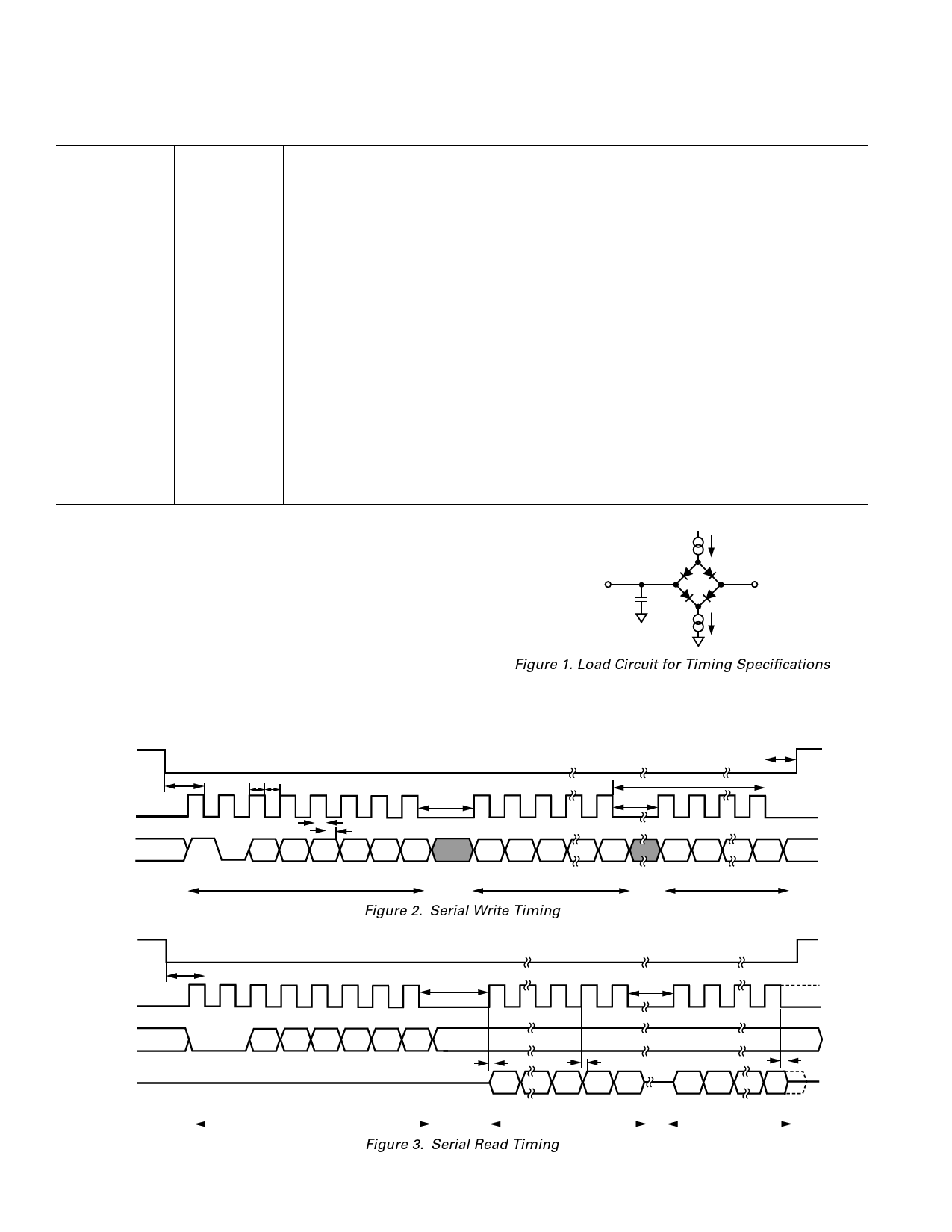
Figure 1. Load Circuit for Timing Specifications
CS
SCLK
DIN
CS
SCLK
DIN
DOUT
t1
1
t2 t3
t7
t4
t5
0 A5 A4 A3 A2 A1 A0
COMMAND BYTE
t7
DB7
DB0
MOST SIGNIFICANT BYTE
Figure 2. Serial Write Timing
t8
t6
DB7
DB0
LEAST SIGNIFICANT BYTE
t1
t9
t10
0 0 A5 A4 A3 A2 A1 A0
t11
DB7
t12
DB0
COMMAND BYTE
MOST SIGNIFICANT BYTE
Figure 3. Serial Read Timing
DB7
t13
DB0
LEAST SIGNIFICANT BYTE
–4–
REV. 0
Share Link: 