ADE7754 Ver la hoja de datos (PDF) - Analog Devices
Número de pieza
componentes Descripción
Fabricante
ADE7754 Datasheet PDF : 44 Pages
| |||
ADE7754
ALIASING EFFECTS
IMAGE
FREQUENCIES
SAMPLING
FREQUENCY
0
2
417
833
FREQUENCY (kHz)
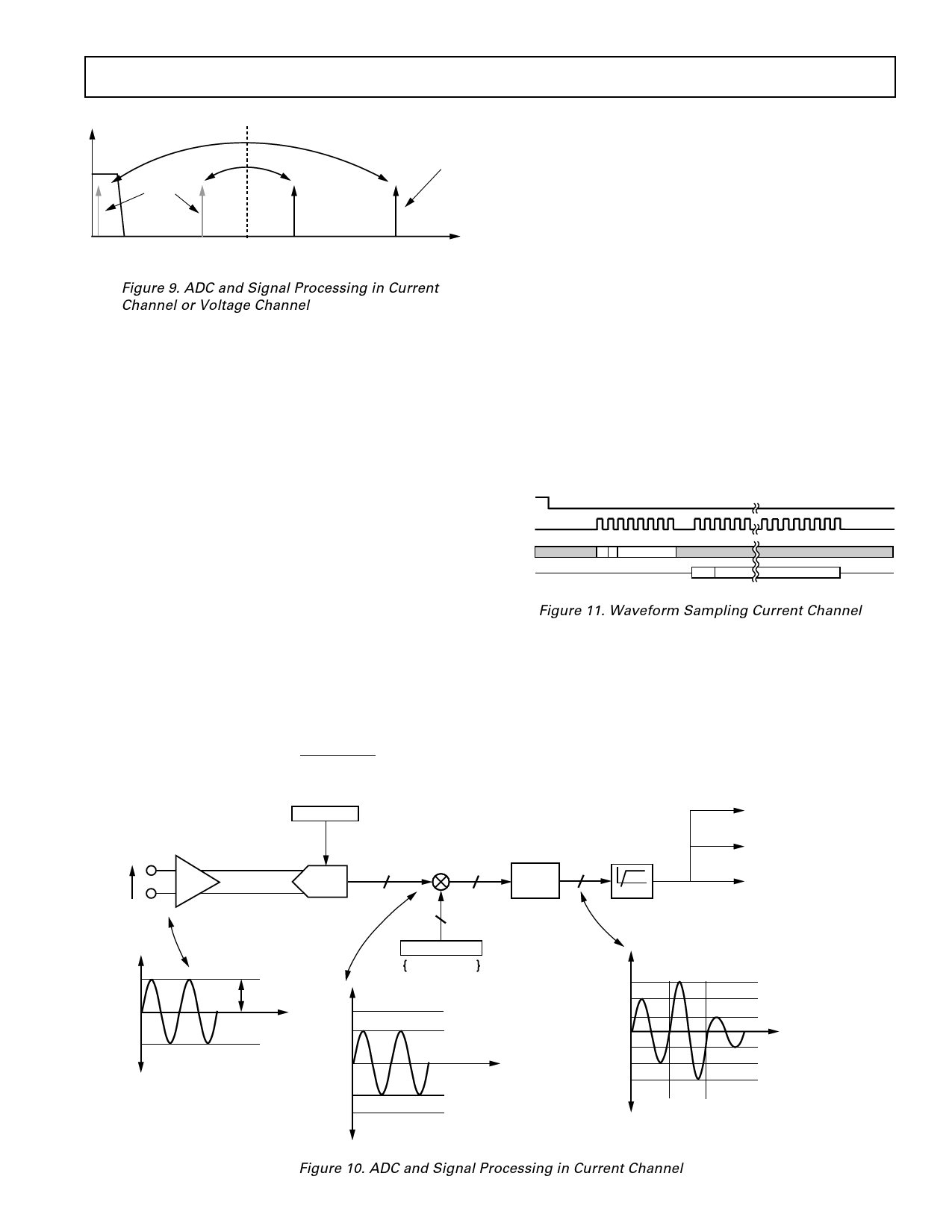
Figure 9. ADC and Signal Processing in Current
Channel or Voltage Channel
CURRENT CHANNEL ADC
Figure 10 shows the ADC and signal processing chain for the
input IA of the current channels (which are the same for IB and
IC). In waveform sampling mode, the ADC outputs are signed
twos complement 24-bit data-word at a maximum of 26 kSPS
(kilo samples per second). The output of the ADC can be
scaled by ± 50% by using the APGAINs register. While the
ADC outputs are 24-bit twos complement value, the maximum
full-scale positive value from the ADC is limited to 400000h
(+4,194,304d). The maximum full-scale negative value is lim-
ited to C00000h (–4,194,304d). If the analog inputs are
overranged, the ADC output code clamps at these values. With
the specified full-scale analog input signal of ± 0.5 V, the ADC
produces an output code between D70A3Eh (–2,684,354) and
28F5C2h (+2,684,354), as illustrated in Figure 10, which also
shows a full-scale voltage signal being applied to the differential
inputs IAP and IAN.
Current Channel ADC Gain Adjust
The ADC gain in each phase of the current channel can be
adjusted using the multiplier and active power gain register
(AAPGAIN[11:0], BAPGAIN, and CAPGAIN). The gain of the
ADC is adjusted by writing a twos complement 12-bit word to
the active power gain register. The following expression shows
how the gain adjustment is related to the contents of that register:
Code
= ADC
×
1 +
AAPGAIN
212
For example, when 7FFh is written to the active power gain
register, the ADC output is scaled up by 50%: 7FFh = 2047d,
2047/212 = 0.5. Similarly, 800h = –2047d (signed twos comple-
ment) and ADC output is scaled by –50%. These two examples
are illustrated in Figure 10.
Current Channel Sampling
The waveform samples of the current channel inputs may also
be routed to the waveform register (wavmode register to select
the speed and the phase) to be read by the system master
(MCU). The active energy and apparent energy calculation remains
uninterrupted during waveform sampling.
When in waveform sample mode, one of four output sample
rates may be chosen using Bits 3 and 4 of the WAVMODE
register (DTRT[1:0] mnemonic). The output sample rate
may be 26.0 kSPS, 13.0 kSPS, 6.5 kSPS, or 3.3 kSPS. See the
Waveform Mode Register section. By setting the WSMP bit in
the interrupt enable register to Logic 1, the interrupt request
output IRQ will go active low when a sample is available. The
timing is shown in Figure 11. The 24-bit waveform samples are
transferred from the ADE7754 one byte (eight bits) at a time,
with the most significant byte shifted out first.
IRQ
SCLK
DIN
READ FROM WAVEFORM
0 0 09h
DOUT
SGN
CURRENT CHANNEL DATA – 24 BITS
Figure 11. Waveform Sampling Current Channel
The interrupt request output IRQ stays low until the interrupt
routine reads the reset status register. See the Interrupt section.
Note that if the WSMP bit in the interrupt enable register is not
set to Logic 1, no data is available in the waveform register.
REFERENCE
CURRENT RMS
CALCULATION
؋1, ؋2, ؋4
IAP
GAIN[1:0]
VIN
IAN
PGA1
ADC
MULTIPLIER
1
1
DIGITAL LPF
24
SINC3
12
HPF
WAVEFORM SAMPLE
REGISTER
ACTIVE AND REACTIVE
POWER CALCULATION
VIN
0V
ANALOG
INPUT
RANGE
REV. 0
100% FS
0.5V/GAIN1
400000h
28F5C2h
000000h
D70A3Eh
C00000h
800h–7FFh
AAPGAIN[11:0]
+100% FS
–100% FS
ADC OUTPUT
WORD RANGE
CHANNEL 1
3D70A3h
28F5C2h
147AE1h
00000h
EB851Fh
D70A3Eh
C28F5Dh
000h 7FFh 800h
Figure 10. ADC and Signal Processing in Current Channel
–11–
+ 150% FS
+ 100% FS
+ 50% FS
AAPGAIN[11:0]
– 50% FS
– 100% FS
– 150% FS
Share Link: 