ADD8616A8A-75BA Ver la hoja de datos (PDF) - A-Data Technology
Número de pieza
componentes Descripción
Fabricante
ADD8616A8A-75BA Datasheet PDF : 9 Pages
| |||
A-Data
ADD8616A8A
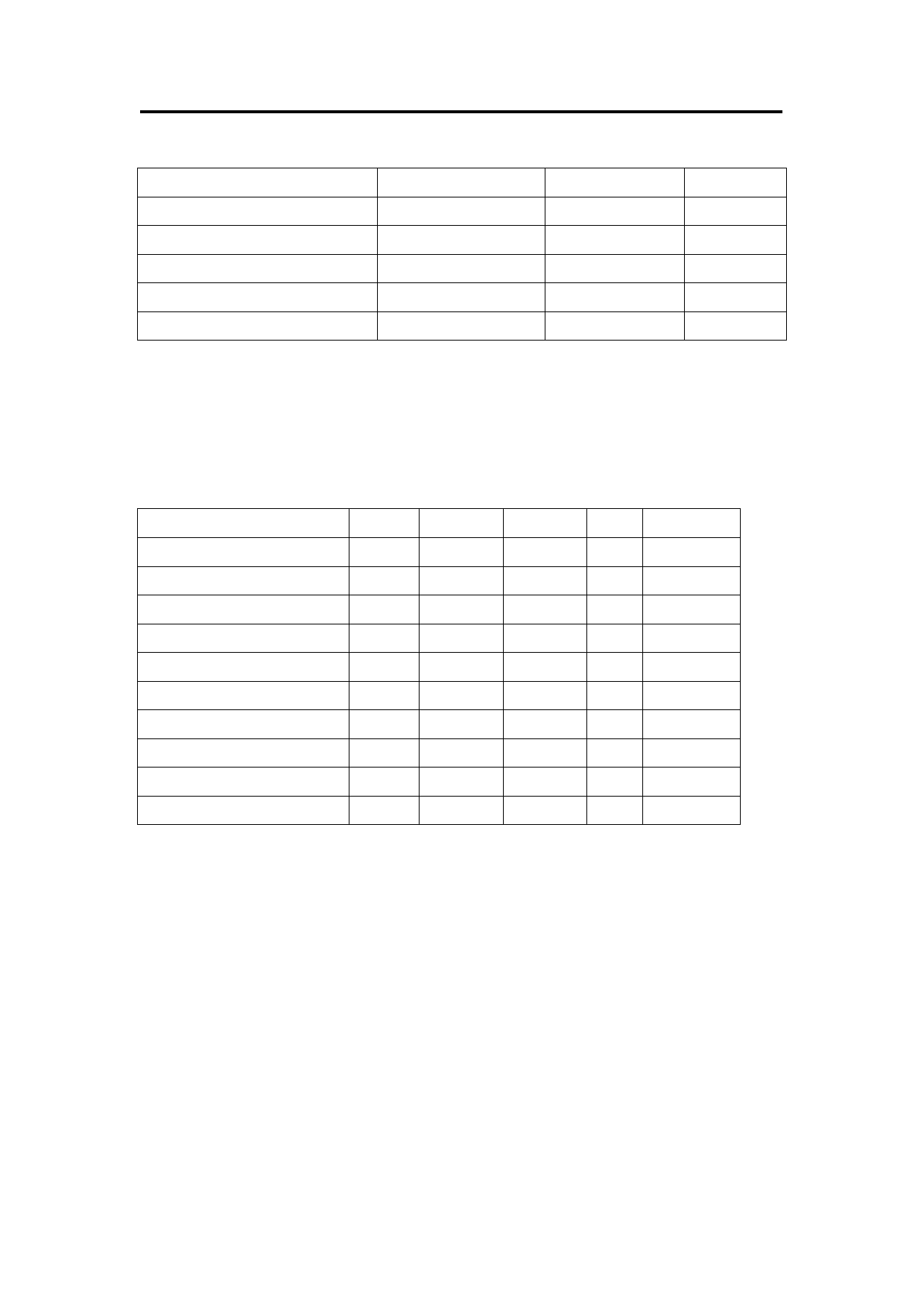
Absolute Maximum Ratings
Parameter
Symbol
Value
Unit
Voltage on any pin relative to Vss
VIN, Vout
-0.3 ~ VDDQ+0.3
V
Voltage on VDD supply relative to Vss
VDD, VDDQ
-0.3 ~ 3.6
V
Storage temperature
TSTG
-55 ~ +150
℃
Power dissipation
PD
1
W
Short circuit current
IOUT
50
mA
Note : Permanent device damage may occur if ABSOLUTE MAXIMUM RATING are exceeded.
Functional operation should be restricted to recommended operating condition.
Exposure to higher than recommended voltage for extended periods of time could affect device reliability.
DC Operating Condition
Voltage referenced to Vss = 0V, TA = 0 to 70 ℃
Parameter
Symbol
Min
Max
Unit
Note
Supply voltage
VDD
2.3
2.7
V
Supply voltage
VDDQ
2.3
VDD
1
Input logic high voltage
VIH
VREF+0.15 VDDQ+0.3
V
Input logic low voltage
VIL
-0.3
VREF-0.15
V
2
Differential Clock DC Input voltage
VICK
-0.3
VDDQ+0.3
V
Input Differential CLK&/CLK voltage
VID
0.7
VDDQ+0.6
V
Input leakage current
IIL
-5
5
uA
3
Output leakage current
IOL
-5
5
uA
4
Reference Voltage
VREF
0.49* VDDQ 0.51* VDDQ
V
Termination Voltage
VTT
VREF-0.04 VREF+0.04
V
5
Note : 1. VDDQ must not exceed the level of VDDQ.
2.VIL(min)=-0.9V with a pulse width ≦ 5ns .
3.Any input 0V ≦ VIN ≦ 3.6V, all other pins are not under test = 0V.
4.Dout is disabled, 0V ≦ VOUT ≦ 2.7V.
5. VREF is expected to be equal to 0.5* VDDQ of the transmitting device, and to track variations in the DC level of
the same. Peak to peak noise on VREF may not exceed ±2% of the DC value.
Rev 2 April, 2002
4
Share Link: 