ADCMP566 Ver la hoja de datos (PDF) - Analog Devices
Número de pieza
componentes Descripción
Fabricante
ADCMP566 Datasheet PDF : 16 Pages
| |||
ADCMP566
PIN CONFIGURATION AND FUNCTION DESCRIPTIONS
GND 1
–INA 2
+INA 3
VCC 4
VCC 5
+INB 6
–INB 7
GND 8
PIN 1
INDICATOR
ADCMP566
TOP VIEW
(Not to Scale)
24 VEE
23 NC
22 VEE
21 VCC
20 VCC
19 VEE
18 NC
17 VEE
NC = NO CONNECT
03633-0-002
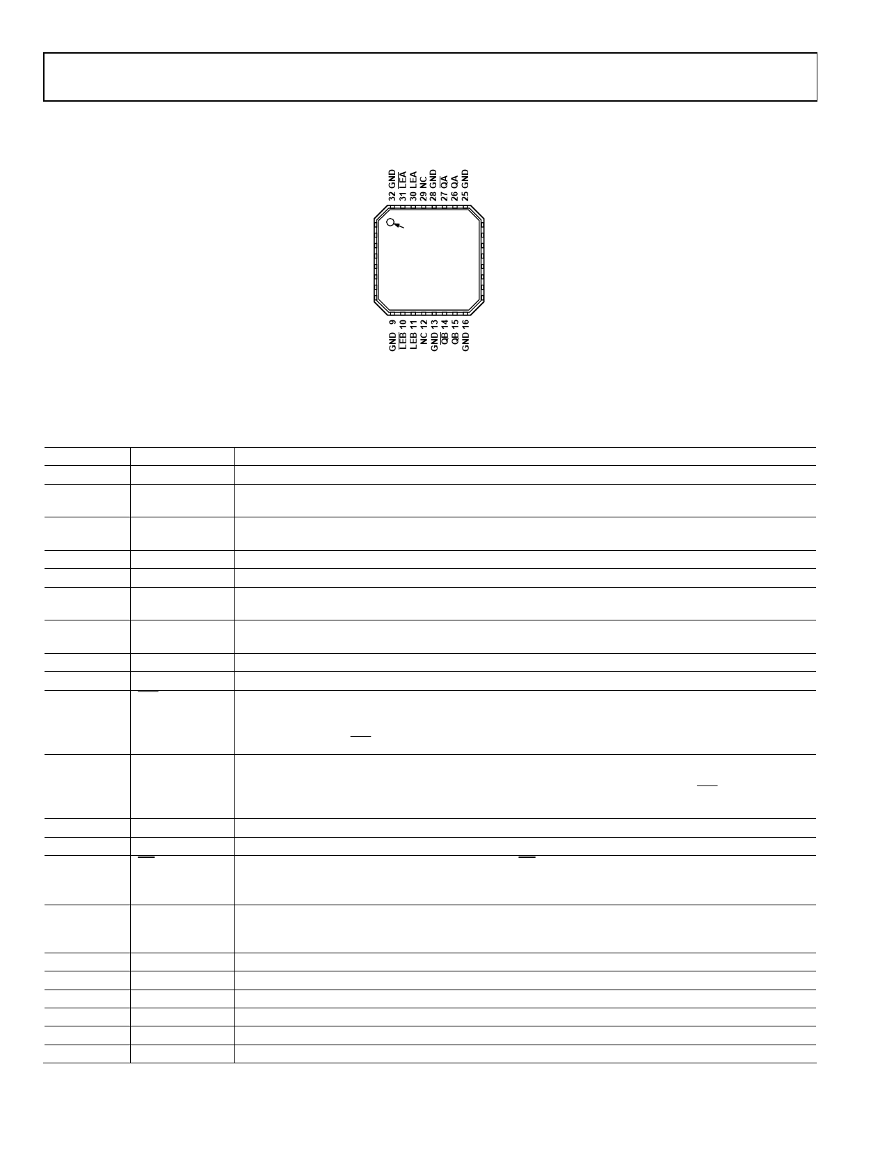
Figure 2. ADCMP566 Pin Configuration
Table 3. ADCMP566 Pin Descriptions
Pin No.
Mnemonic
Function
1
GND
Analog Ground
2
−INA
Inverting analog input of the differential input stage for Channel A. The inverting A input must be driven
in conjunction with the noninverting A input.
3
+INA
Noninverting analog input of the differential input stage for Channel A. The noninverting A input must
be driven in conjunction with the inverting A input.
4
VCC
Positive Supply Terminal
5
VCC
Positive Supply Terminal
6
+INB
Noninverting analog input of the differential input stage for Channel B. The noninverting B input must
be driven in conjunction with the inverting B input.
7
−INB
Inverting analog input of the differential input stage for Channel B. The inverting B input must be driven
in conjunction with the noninverting B input.
8
GND
Analog Ground
9
GND
Analog Ground
10
LEB
One of two complementary inputs for Channel B Latch Enable. In the compare mode (logic low), the
output will track changes at the input of the comparator. In the latch mode (logic high), the output will
reflect the input state just prior to the comparator’s being placed in the latch mode. LEB must be driven
in conjunction with LEB.
11
LEB
One of two complementary inputs for Channel B Latch Enable. In the compare mode (logic high), the
output will track changes at the input of the comparator. In the latch mode (logic low), the output will
reflect the input state just prior to the comparator’s being placed in the latch mode. LEB must be driven
in conjunction with LEB.
12
NC
No Connect. Leave pin unconnected.
13
GND
Digital Ground
14
QB
One of two complementary outputs for Channel B. QB will be at logic low if the analog voltage at the
noninverting input is greater than the analog voltage at the inverting input (provided the comparator is
in the compare mode). See the LEB description (Pin 11) for more information.
15
QB
One of two complementary outputs for Channel B. QB will be at logic high if the analog voltage at the
noninverting input is greater than the analog voltage at the inverting input (provided the comparator is
in the compare mode). See the LEB description (Pin 11) for more information.
16
GND
Digital Ground
17
VEE
Negative Supply Terminal
18
NC
No Connect. Leave pin unconnected.
19
VEE
Negative Supply Terminal
20
VCC
Positive Supply Terminal
21
VCC
Positive Supply Terminal
Rev. 0 | Page 6 of 16
Share Link: 