ADC912A Ver la hoja de datos (PDF) - Analog Devices
Número de pieza
componentes Descripción
Fabricante
ADC912A Datasheet PDF : 16 Pages
| |||
ADC912A
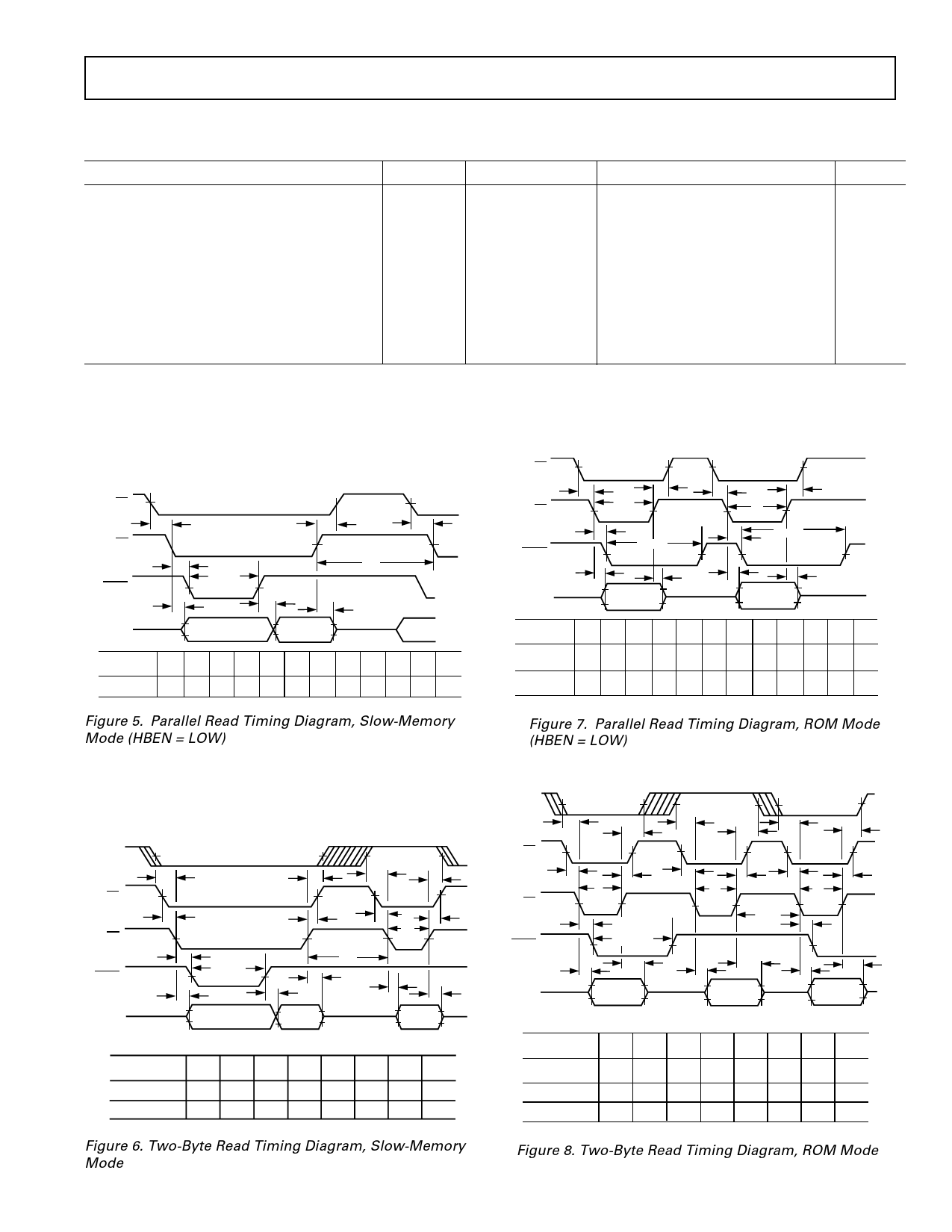
TIMING CHARACTERISTICS1, 2 (VDD = +5 V ؎ 5%, VSS = –11.4 V to –15.75 V, VREFIN = –5 V, Analog Input 0 V to 10 V;
External fCLK = 1.25 MHz; –40؇C to +85؇C applies to ADC912A/F unless otherwise noted. See Figures 5 to 8.)
Parameter
Symbol
Conditions
Min
Typ
Max
Unit
CS to RD Setup Time
t1
RD to BUSY Propagation Delay
t2
Data Access Time after READ
t33
Read Pulsewidth
t43
CS to RD Hold Time
t5
New Data Valid after BUSY
t63
Bus Disconnect Time
t7
HBEN to RD Setup Time
t8
HBEN to RD Hold Time
t9
Delay between Successive Read Operations
t10
0
ns
150
ns
CL = 100 pF
65
125
ns
90
ns
0
ns
CL = 100 pF
–30
0
ns
20
60
90
ns
20
ns
20
ns
350
250
ns
NOTES
1Guaranteed by design.
2All input control signals are specified with tR = tF = 5 ns (10% to 90% of 5 V) and timed from a voltage level of 1.6 V.
3t3, t4, and t6 are measured with the load circuits of Figure 3 and timed for and output to cross 0.8 V or 2.4 V.
4t7 is the time required for the data lines to change 0.5 V when loaded with the circuits of Figure 4.
Specifications subject to change without notice.
CS
TIMING DIAGRAMS
CS
t1
RD
t5
t1
BUSY
DATA
t2
tCONV
t10
t3
t6
t7
OLD DATA
NEW DATA
DB11 – DB0
DB11 – DB0
RD
BUSY
DATA
t1
t5
t4
t2
tCONV
t3
t7
OLD DATA
DB11 – DB0
t1
t5
t4
t2
tCONV
t3
t7
NEW DATA
DB11 – DB0
DATA
OUTPUTS
D11
D10
D9
D8 D7
D6 D5 D4 D3/11 D2/10 D1/9 D0/8
DATA
OUTPUTS
D11
D10
D9
D8 D7
D6 D5 D4 D3/11 D2/10 D1/9 D0/8
READ DB11 DB10 DB9 DB8 DB7 DB6 DB5 DB4 DB3 DB2 DB1 DB0
FIRST READ
(OLD DATA)
DB11
DB10
DB9
DB8
DB7
DB6
DB5
DB4
DB3
DB2 DB1
DB0
SECOND
READ
DB11
DB10
DB9
DB8
DB7
DB6
DB5
DB4
DB3
DB2 DB1
DB0
Figure 5. Parallel Read Timing Diagram, Slow-Memory
Mode (HBEN = LOW)
Figure 7. Parallel Read Timing Diagram, ROM Mode
(HBEN = LOW)
HBEN
t8
CS
t9
t8
t9
t1
RD
t5
t1
t5
t4
BUSY
DATA
t2
t3
DATA
OUTPUTS
tCONV
OLD DATA
DB7 – DB0
D7
D6
t10
t7
t6
t3
t7
NEW DATA
DB7 – DB0
NEW DATA
DB11 – DB8
D5
D4
D3/11 D2/10 D1/9
D0/8
FIRST READ DB7
SECOND READ LOW
DB6
LOW
DB5 DB4
LOW LOW
DB3 DB2
DB11 DB10
DB1
DB9
DB0
DB8
HBEN
CS
RD
BUSY
DATA
t8
t9
t1
t5
t4
t2
tCONV
t3
t7
OLD DATA
DB7 – DB0
t8
t9
t8
t9
t1
t5
t4
t1
t5
t4
t10
t2
t3
t7
NEW DATA
DB11 – DB8
t3
t7
NEW DATA
DB7 – DB0
DATA
OUTPUTS
D7
FIRST READ
(OLD DATA)
DB7
SECOND READ LOW
THIRD READ DB7
D6
DB6
LOW
DB6
D5
DB5
LOW
DB5
D4
DB4
LOW
DB4
D3/11 D2/10
DB3 DB2
DB11 DB10
DB3 DB2
D1/9
DB1
DB9
DB1
D0/8
DB0
DB8
DB0
Figure 6. Two-Byte Read Timing Diagram, Slow-Memory
Mode
Figure 8. Two-Byte Read Timing Diagram, ROM Mode
REV. B
–3–
Share Link: 