ADADC80-Z-12 Ver la hoja de datos (PDF) - Analog Devices
Número de pieza
componentes Descripción
Fabricante
ADADC80-Z-12 Datasheet PDF : 12 Pages
| |||
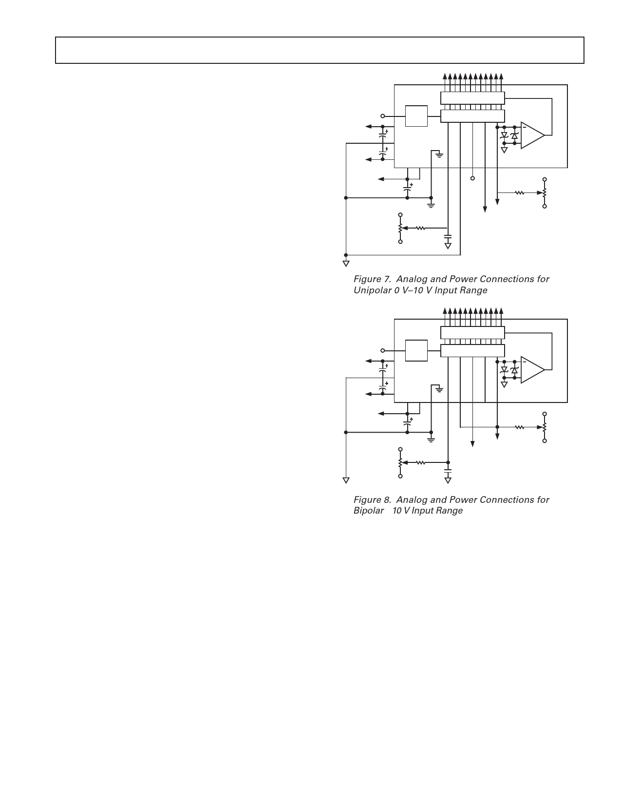
CALIBRATION
External ZERO ADJ and GAIN ADJ potentiometers, connected
as shown in Figures 7 and 8, are used for device calibration.
To prevent interaction of these two adjustments, zero is always
adjusted first and then gain. Zero is adjusted with the analog input
near the most negative end of the analog range (0 for unipolar
and –FS for bipolar input ranges). Gain is adjusted with the
analog input near the most positive end of the analog range.
0 to 10 V Range
Set analog input to +1 LSB = 0.0024 V. Adjust zero for
digital output = 111111111110. Zero is now calibrated. Set
analog input to +FSR – 2 LSB = 9.9952 V. Adjust gain for
000000000001 digital output code. Full-scale (gain) is now
calibrated. For half-scale calibration check set analog input to
5.0000 V; digital output code should be 011111111111.
–10 V to +10 V Range
Set analog input to –9.9951 V, adjust zero for 111111111110
digital output (complementary offset binary) code. Set ana-
log input to +9.9902 V, adjust gain for 000000000001
digital output (complementary offset binary) code. For
half-scale calibration check, set analog input to 0.0000 V;
digital output (complementary offset binary) code should be
011111111111.
Other Ranges
Representative digital coding for 0 V to +10 V and –10 V to +10 V
ranges is given above. Coding relationships and calibration
points for 0 V to +5 V, –2.5 V to +2.5 V, and –5 V to +5 V ranges
can be found by halving the corresponding code equivalents
listed for the 0 V to +10 V and –10 V to +10 V ranges, respectively.
Zero and full-scale calibration can be accomplished to a precision
of approximately ±1/4 LSB using the static adjustment procedure
described above. By summing a small sine- or triangular-wave
voltage with the signal applied to the analog input, the output
can be cycled through each of the calibration codes of interest
to more accurately determine the center (or end points) of each
discrete quantization level. A detailed description of this
dynamic calibration technique is presented in A/D Conversion Notes,
D. Sheingold, Analog Devices, Inc., 1977, Part II, Chapter 3.
AD ADC80
+15V
24
REF
17
SAR
DAC
15
COMP
–15V
+5V
25
79
10 16 12 14 13 11
AD ADC80
–15V
1.8M⍀
10k⍀
–15V
10k⍀
10M⍀
0.01F
+15V
ANALOG
INPUT
+15V
Figure 7. Analog and Power Connections for
Unipolar 0 V–10 V Input Range
+15V
24
REF
17
SAR
DAC
15
COMP
–15V
+5V
25
79
10 16 12 14 13 11
AD ADC80
–15V
1.8M⍀
10k⍀
–15V
10k⍀
10M⍀
0.01F
+15V
ANALOG
INPUT
+15V
Figure 8. Analog and Power Connections for
Bipolar ±10 V Input Range
REV. D
–9–
Share Link: 