ADADC80-Z-12 Ver la hoja de datos (PDF) - Analog Devices
Número de pieza
componentes Descripción
Fabricante
ADADC80-Z-12 Datasheet PDF : 12 Pages
| |||
AD ADC80
Binary (BIN)
Output
Analog Input
Voltage Range
Code
Designation
One Least
Significant
Bit (LSB)
Table III. Input Voltages and Code Definitions
Defined As:
FSR
2n
n=8
n = 10
n = 12
؎10 V
COB1
or CTC2
20 V
2n
78.13 mV
19.53 mV
4.88 mV
؎5 V
COB1
or CTC2
10 V
2n
39.06 mV
9.77 mV
2.44 mV
؎2.5 V
COB1
or CTC2
5V
2n
19.53 mV
4.88 mV
1.22 mV
0 V to ؉10 V
CSB3
10 V
2n
39.06 mV
9.77 mV
2.44 mV
0 V to ؉5 V
CSB3
5V
2n
19.53 mV
4.88 mV
1.22 mV
Transition Values
MSB LSB
000 . . . . 0004
011 . . . . 111
111 . . . . 110
+Full Scale
Midscale
–Full Scale
10 V – 3/2 LSB 5 V – 3/2 LSB 2.5 V – 3/2 LSB 10 V – 3/2 LSB
0
0
0
5V
–10 V + 1/2 LSB –5 V + 1/2 LSB –2.5 V + 1/2 LSB 0 V + 1/2 LSB
5 V – 3/2 LSB
2.5 V
0 V + 1/2 LSB
NOTES
1COB = Complementary Offset Binary
2CTC = Complementary Twos Complement—obtained by using the complement of the most significant bit ( MSB). MSB is available on Pin 8.
3CSB = Complementary Straight Binary
4Voltages given are the nominal value for transition to the code specified.
OFFSET ADJUSTMENT
The zero adjust circuit consists of a potentiometer connected
across ± VS with its slider connected through a 1.8 MΩ resistor to
Comparator Input Pin 11 for all ranges. As shown in Figure 3,
the tolerance of this fixed resistor is not critical, and a carbon
composition type is generally adequate. Using a carbon com-
position resistor with a –1200 ppm/°C tempco contributes a
worst-case offset tempco of 8 ϫ 244 ϫ 10–6 ϫ 1200 ppm/°C =
2.3 ppm/°C of FSR, if the OFFSET ADJ potentiometer is set at
either end of its adjustment range. Since the maximum offset
adjustment required is typically no more than ± 4 LSB, use of a
carbon composition offset summing resistor typically contributes
no more than 1 ppm/°C of FSR offset tempco.
+15V
10k⍀
TO
100k⍀
–15V
1.8M⍀ 11
AD ADC80
Figure 3. Offset Adjustment Circuit
An alternate offset adjust circuit, which contributes negligible
offset tempco if metal film resistors (tempco <100 ppm/°C) are
used, is shown in Figure 4.
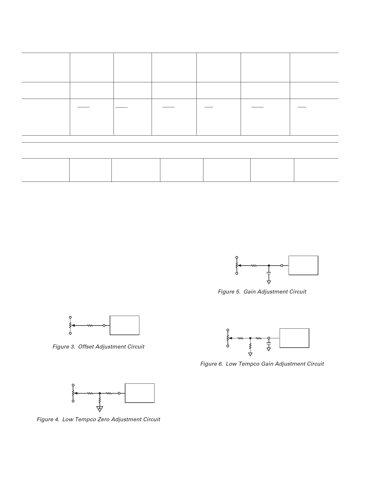
GAIN ADJUSTMENT
The gain adjust circuit consists of a potentiometer connected
across ± VS with its slider connected through a 10 MΩ resistor
to the gain adjust Pin 16, as shown in Figure 5.
+15V
GAIN
ADJUST
10k⍀
TO
100k⍀
–15V
10M⍀
16
0.01F
AD ADC80
Figure 5. Gain Adjustment Circuit
An alternate gain adjust circuit, which contributes negligible
gain tempco if metal film resistors (tempco <100 ppm/°C) are
used, is shown in Figure 6.
+15V
10k⍀
TO
100k⍀
–15V
270k⍀
MF
6.8k⍀
270k⍀
MF 16
0.1F
AD ADC80
Figure 6. Low Tempco Gain Adjustment Circuit
+15V
OFFSET
ADJUST
10k⍀
TO
100k⍀
–15V
180k⍀ 180k⍀
MF
MF 11
22k⍀
MF
AD ADC80
Figure 4. Low Tempco Zero Adjustment Circuit
In either zero adjust circuit, the fixed resistor connected to
Pin 11 should be located close to this pin to keep the Pin 11
connection runs short. Comparator Input Pin 11 is quite sensi-
tive to external noise pickup.
–8–
REV. D
Share Link: 