ADADC80-Z-12 Ver la hoja de datos (PDF) - Analog Devices
Número de pieza
componentes Descripción
Fabricante
ADADC80-Z-12 Datasheet PDF : 12 Pages
| |||
AD ADC80
DIGITAL OUTPUT DATA
Parallel data from TTL storage registers is in negative true
form. Parallel data output coding is complementary binary
for unipolar ranges and either complementary offset binary
or complementary twos complement binary, depending on
whether Bit 1 (Pin 6) or its logical inverse Bit 1 (Pin 8) is used
as the MSB. Parallel data becomes valid approximately 40 ns
before the STATUS flag returns to Logic 0, permitting
parallel data transfer to be clocked on the 1 to 0 transition of
the STATUS flag.
Parallel data outputs change state on positive-going clock edges.
There are 13 negative-going clock edges in the complete 12-bit
conversion cycle, as shown in Figure 1. The first edge shifts an
invalid bit into the register, which is shifted out on the 13th
negative-going clock edge.
Short Cycle Input
A short cycle input, Pin 21, permits the timing cycle shown in
Figure 1 to be terminated after any number of desired bits has
been converted, permitting somewhat shorter conversion times
in applications not requiring full 12-bit resolution. When 10-bit
resolution is desired, Pin 21 is connected to Bit 11, output
Pin 28. The conversion cycle then terminates, and the STATUS
flag resets after the Bit 10 decision (t10 + 40 ns in timing dia-
gram of Figure 1). Short cycle pin connections and associated
maximum 12-, 10-, and 8-bit conversion times are summarized
in Table I. When 12-bit resolution is required, Pin 21 is con-
nected to 5 V (Pin 9).
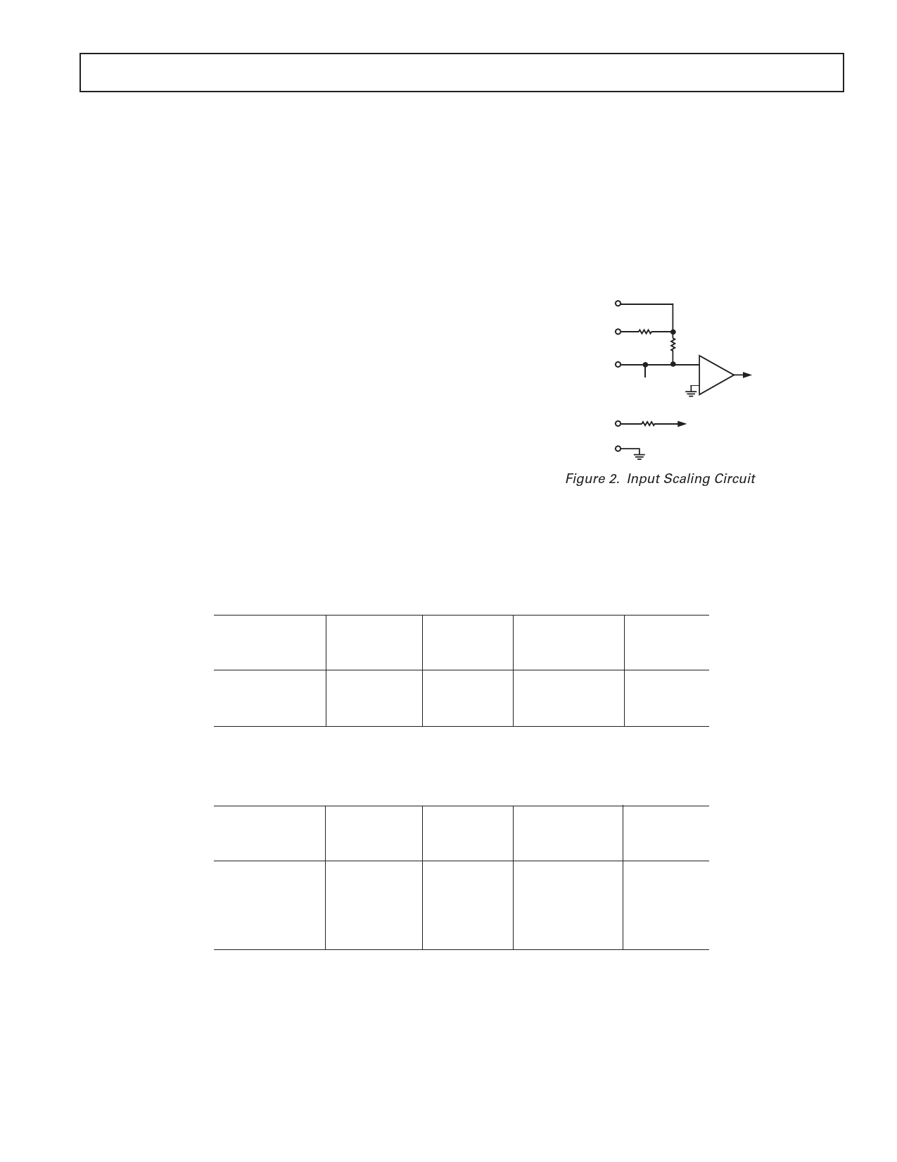
INPUT SCALING
The AD ADC80 input should be scaled as close to the maximum
input signal range as possible to use the maximum signal
resolution of the A/D converter. Connect the input signal as shown
in Table II. See Figure 2 for circuit details.
10V RANGE 13
R2, 5k⍀
20V RANGE 14
R1, 5k⍀
COMP IN 11
FROM D/A
CONVERTER
TO SAR
COMPARATOR
BIPOLAR 12
OFFSET
ANALOG
COMMON
15
6.3k⍀
VREF
Figure 2. Input Scaling Circuit
Connect Short
Cycle Pin 21
to Pin
9
28
30
Table I. Short Cycle Connections
Resolution
Bits
12
10
8
(% FSR)
0.024
0.100
0.390
Maximum
Conversion
Time (s)
25
21
17
Status
Flag
Reset
t12 + 40 ns
t10 + 40 ns
t8 + 40 ns
Input
Signal
Range
± 10 V
±5 V
± 2.5 V
0 V to 5 V
0 V to 10 V
Table II. Input Scaling Connections
Output
Code
COB or CTC
COB or CTC
COB or CTC
CSB
CSB
Connect
Pin 12
to Pin
11
11
11
15
15
Connect
Pin 14
to
Input Signal
Open
Pin 11
Pin 11
Open
Connect
Input
Signal to
14
13
13
13
13
REV. D
–7–
Share Link: 