ADADC80-Z-12 Ver la hoja de datos (PDF) - Analog Devices
Número de pieza
componentes Descripción
Fabricante
ADADC80-Z-12 Datasheet PDF : 12 Pages
| |||
AD ADC80
THEORY OF OPERATION
On receipt of a CONVERT START command, the AD ADC80
converts the voltage at its analog input into an equivalent 12-bit
binary number. This conversion is accomplished as follows: the
12-bit successive-approximation register (SAR) has its 12-bit
outputs connected both to the device bit output pins and to the
corresponding bit inputs of the feedback DAC. The analog input
is successively compared to the feedback DAC output, one bit
at a time (MSB first, LSB last). The decision to keep or reject
each bit is then made at the completion of each bit comparison
period, depending on the state of the comparator at that time.
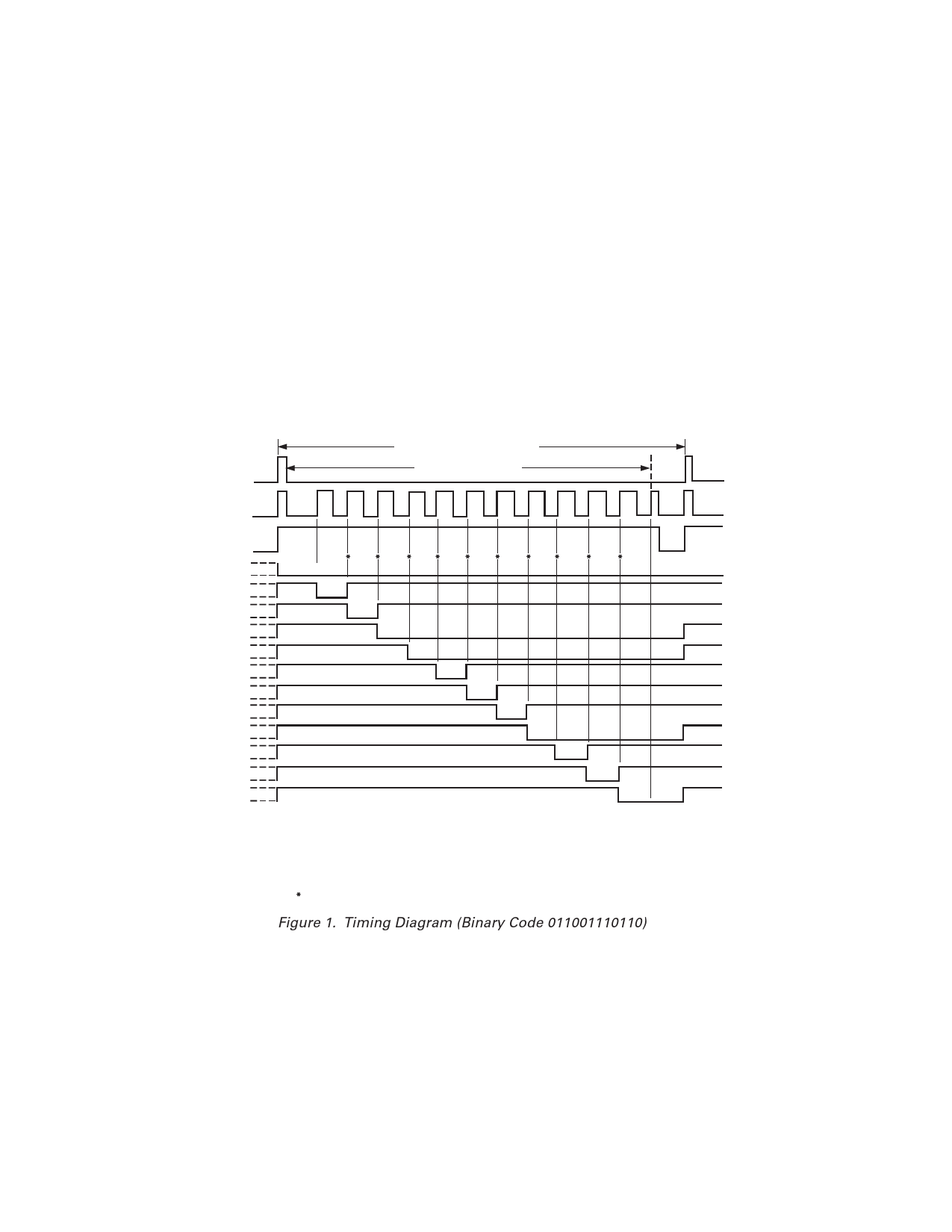
TIMING
The timing diagram is shown in Figure 1. Receipt of a CONVERT
START signal sets the STATUS flag, indicating conversion in
progress. This, in turn, removes the inhibit applied to the gated
clock, permitting it to run through 13 cycles. All SAR parallel
bit and STATUS flip-flops are initialized on the leading edge, and
the gated clock inhibit signal is removed on the trailing edge of
the CONVERT START signal. At time t0, B1 is reset and B2–B12
are set unconditionally. At t1, the Bit 1 decision is made (keep)
and Bit 2 is unconditionally reset. At t2, the Bit 2 decision is
made (keep) and Bit 3 is reset unconditionally. This sequence
continues until the Bit 12 (LSB) decision (keep) is made at t12.
After a 40 ns delay period, the STATUS flag is reset, indicating
that the conversion is complete and the parallel output data is
valid. Resetting the STATUS flag restores the gated clock
inhibit signal, forcing the clock output to the Logic 0 state.
Parallel data bits become valid on the positive-going clock edge
(see Figure 1).
Incorporation of this 40 ns delay guarantees that the parallel
data is valid at the Logic l to 0 transition of the STATUS flag,
permitting parallel data transfer to be initiated by the trailing edge
of the STATUS signal.
CONVERT1
START
INTERNAL
CLOCK
STATUS
MSB
BIT 2
BIT 3
BIT 4
BIT 5
BIT 6
BIT 7
BIT 8
BIT 9
BIT 10
BIT 11
LSB
MAXIMUM THROUGHPUT TIME
CONVERSION TIME2
t0
t1
t2 t3
NOTE
3
0
t4 t5
t6
t7
t8
t9 t10 t11
NOTE
4
t12
1
1
0
0
1
1
1
0
1
1
0
NOTES
1THE CONVERT START PULSEWIDTH IS 100ns MIN AND MUST REMAIN LOW DURING
A CONVERSION; THE CONVERSION IS INITIATED BY THE RISING EDGE OF THE
CONVERT COMMAND
225s FOR 12 BITS AND 21s FOR 10 BITS (MAX)
3MSB DECISION
4LSB DECISION 40ns PRIOR TO THE STATUS GOING LOW
BIT DECISIONS
Figure 1. Timing Diagram (Binary Code 011001110110)
–6–
REV. D
Share Link: 