ADADC80-Z-12 Ver la hoja de datos (PDF) - Analog Devices
Número de pieza
componentes Descripción
Fabricante
ADADC80-Z-12 Datasheet PDF : 12 Pages
| |||
AD ADC80
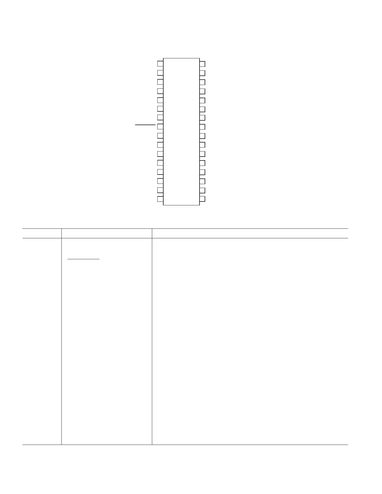
PIN CONFIGURATION
Pin No.
1–6
7
8
9
10
11
12
13
14
15
16
17
18
19
20
21
22
23
24
25
26
27–32
BIT 6 1
BIT 5 2
BIT 4 3
BIT 3 4
BIT 2 5
BIT 1 (MSB) 6
5V ANALOG
SUPPLY 7
BIT 1 (MSB) 8
5V DIGITAL
SUPPLY 9
DIGITAL GND 10
COMPARATOR IN 11
BIPOLAR
OFFSET OUT
12
10V SPAN IN 13
20V SPAN IN 14
ANALOG GND 15
GAIN ADJUST 16
AD ADC80
32 BIT 7
31 BIT 8
30 BIT 9
29 BIT 10
28 BIT 11
27 BIT 12 (LSB)
26 NC
25 –15V OR –12V
24 REF OUT (6.3V)
23 CLOCK OUT
22 STATUS
21 SHORT CYCLE
20 CLOCK INHIBIT
19 EXTERNAL CLOCK IN
18 CONVERT START
17 15V OR 12V
NC = NO CONNECT
Mnemonic
BIT 6–BIT 1 (MSB)
5 V ANALOG SUPPLY
BIT 1 (MSB)
5 V DIGITAL SUPPLY
DIGITAL GND
COMPARATOR IN
BIPOLAR OFFSET OUT
10 V SPAN IN
20 V SPAN IN
ANALOG GND
GAIN ADJUST
15 V OR 12 V
CONVERT START
EXTERNAL CLOCK IN
CLOCK INHIBIT
SHORT CYCLE
STATUS
CLOCK OUT
REF OUT (6.3 V)
–15 V OR –12 V
NC
BIT 12 (LSB)–BIT 7
PIN FUNCTION DESCRIPTIONS
Function
Digital Outputs
Analog Positive Supply (Nominally ± 0.25 V)
MSB Inverted Digital Output
Digital Positive Supply (Nominally ± 0.25 V)
Digital Ground
Offset Adjust
Bipolar Offset Output
Analog Input 10 V Signal Range
Analog Input 20 V Signal Range
Analog Ground
Gain Adjust
Analog Positive Supply (Nominally ± 1.0 V for +15 V or ± 0.6 V for +12 V)
Enables Conversion
External Clock Input
Clock Inhibit
Shortens Conversion Cycle to Desired Resolution
Logic High, ADC Converting/Logic Low, ADC Data Valid
Internal Clock Output
6.3 V Reference Output
Analog Negative Supply (Nominally ± 1.0 V for –15 V or ± 0.6 V for –12 V)
No Connection
Digital Outputs
–4–
REV. D
Share Link: 