TDD25-12S3 Ver la hoja de datos (PDF) - CHINFA ELECTRONICS
Número de pieza
componentes Descripción
Fabricante
TDD25-12S3 Datasheet PDF : 4 Pages
| |||
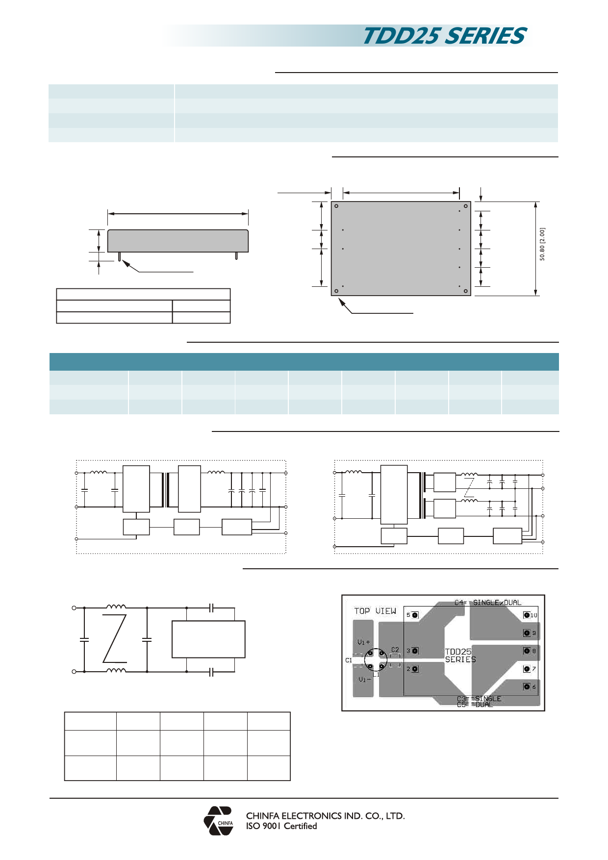
PHYSICAL CHARACTERISTICS
Case size
76.2 x 50.8 x 12 mm ( 3 x 2 x 0.47 inches )
Case material
Plastic base / Metal case
Weight
105 g
Potting material
Epoxy
MECHANISM & PIN CONFIGURATION
mm [inch]
6.35 [0.25]
76.20 [3.00]
15.24 [0.60]
12.00 [0.47]
6.00 [0.24]
DIA 1.00 [0.04]
10.16 [0.40]
20.32 [0.80]
GENERAL TOLERANCE
0.00[0.00] - 30.00[1.18]
±0.30[0.01]
30.00[1.18] - 120.00[4.72]
±0.50[0.02]
PIN ASSIGNMENT
GENERAL
PIN NO.
2
3
SINGLE
Vi -
Vi+
DUAL
Vi -
Vi+
5
ON / OFF
ON / OFF
6
N. C.
Vo -
TDD25 SERIES
SINGLE & DUAL OUTPUT
63.50 [2.50]
6
2
7
3
8
9
5
10
BURL AT 4 CORNER
BOTTOM VIEW
5.08 [0.20]
10.16 [0.40]
10.16 [0.40]
10.16 [0.40]
10.16 [0.40]
7
8
9
10
N. C.
Vo -
Vo +
Trim
N. C.
com
Vo +
Trim
CIRCUIT SCHEMATIC
‧Block diagram for TDD25 series with single output
Vi +
Vi -
ON / OFF
Switching
Device
Rectifier
PWM
Controller
Opto -
Isolation
Reference &
Error Amp.
‧Block diagram for TDD25 series with dual output
Vo +
Vi +
Vo -
Vi -
Trim
ON / OFF
Switching
Device
PWM
Controller
Rectifier
Rectifier
Opto -
Isolation
Reference &
Error Amp.
Vo +
com
Vo -
Trim
RECOMMENDED CIRCUIT
‧Recommended filter for EN55022 Class B compliance.
L1
C4
+
Vin +
Vo +
C1
C2
TDD25
Vin -
Vo -
-
C3/C5
‧The components used in the above figure, together with the manufacturer
part numbers for these components, are as follows.
C1
C2
C3/C4/C5
6.8μF / 100V 6.8μF / 100V
TDD25-XXSX MLCC
MLCC
InF / 2KV
MLCC
TDD25-XXDX
6.8μF / 100V
MLCC
6.8μF / 100V
MLCC
2.2nF / 2KV
MLCC
L1
500μH
Command
Chock
500μH
Command
Chock
www.chinfa.com
2014.05.26
‧Recommended EN 55022 Class B filter circuit layout.
sales@chinfa.com
P3
Share Link: 