AD9984AKSTZ-170 Ver la hoja de datos (PDF) - Analog Devices
Número de pieza
componentes Descripción
Fabricante
AD9984AKSTZ-170 Datasheet PDF : 44 Pages
| |||
AD9984A
SPECIFICATIONS
ANALOG INTERFACE CHARACTERISTICS
VD = 1.8 V, VDD = 3.3 V, PVD = 1.8 V, DAVDD = 1.8 V, ADC clock = maximum conversion rate, full temperature range = 0°C to 70°C.
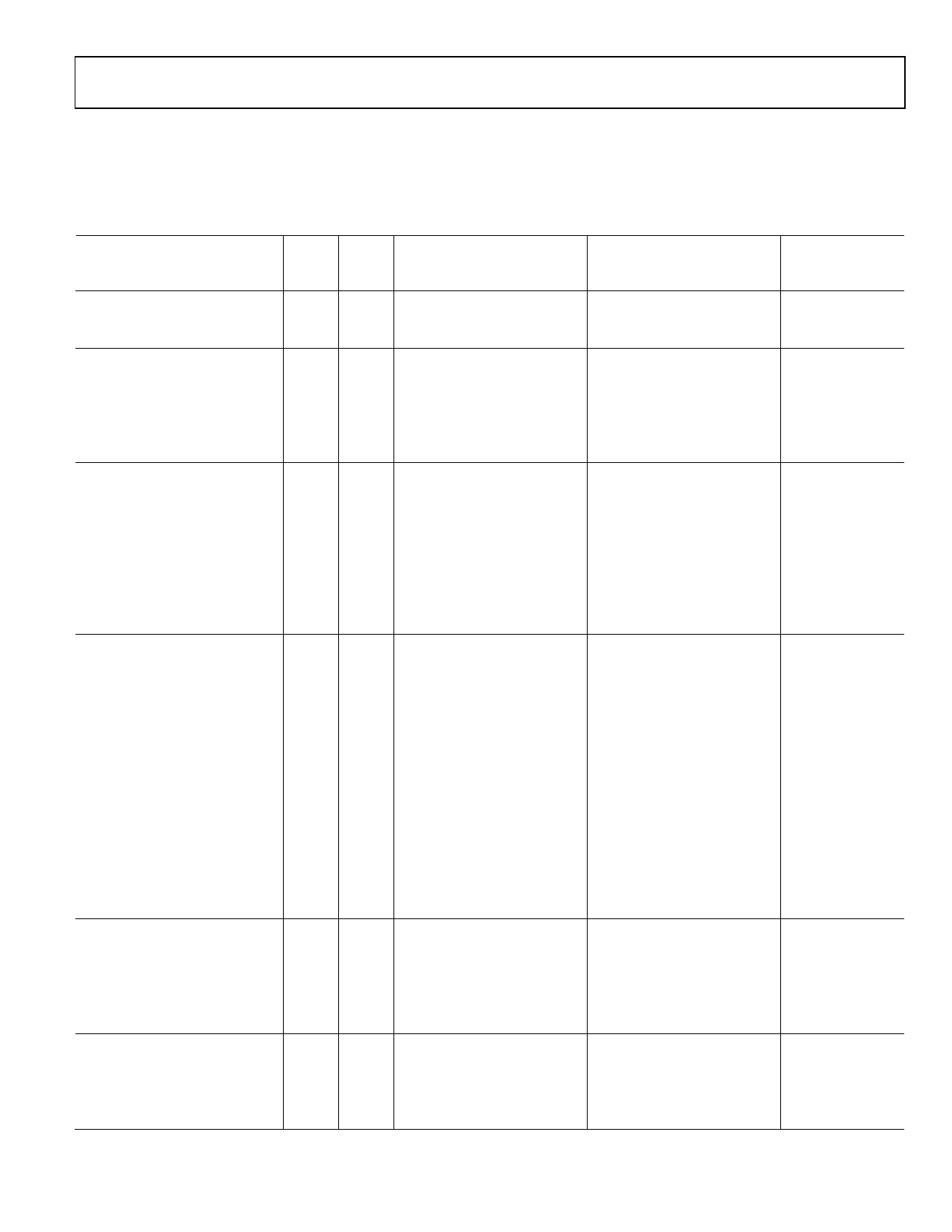
Table 1. Electrical Characteristics
Parameter
RESOLUTION
Number of Bits
LSB Size
DC ACCURACY
Differential Nonlinearity
Integral Nonlinearity
No Missing Codes
ANALOG INPUT
Input Voltage Range
Minimum
Maximum
Gain Tempco
Input Bias Current
Input Full-Scale Matching
Offset Adjustment Range
SWITCHING PERFORMANCE
Maximum Conversion Rate
Minimum Conversion Rate
Clock to Data Skew (tSKEW)
tBUFF
tSTAH
tDHO
tDAL
tDAH
tDSU
tSTASU
tSTOSU
Maximum PLL Clock Rate
Minimum PLL Clock Rate
Sampling Phase Tempco
DIGITAL INPUTS
Input Voltage, High (VIH)
Input Voltage, Low (VIL)
Input Current, High (IIH)
Input Current, Low (IIL)
Input Capacitance
DIGITAL OUTPUTS
Output Voltage, High (VOH)
Output Voltage, Low (VOL)
Duty Cycle (DATACK)
Output Coding
Temp
25°C
Full
25°C
Full
Full
Full
Full
25°C
25°C
Full
Full
Full
Full
Full
Full
Full
Full
Full
Full
Full
Full
Full
Full
Full
Full
Full
Full
Full
Full
Full
25°C
Full
Full
Full
AD9984AKSTZ-140
AD9984AKSTZ-170
Test
AD9984AKCPZ-140
AD9984AKCPZ-170
Level1 Min
Typ Max
Min
Typ Max
Unit
10
0.098
10
0.098
Bits
% of full scale (FS)
I
±0.6 +1.8/−1.0
±0.7 +1.9/−1.0 LSB
VI
+1.9/−1.0
+2.0/−1.0 LSB
I
±2.35 ±7.0
±2.35 ±8.5
LSB
VI
±9.0
±9.0
LSB
VI
GNT2
GNT2
VI
VI
1.0
V
IV
IV
VI
VI
0.5
125
1
1
1
50
0.5
1.0
125
1
1
1
50
V p-p
V p-p
ppm/°C
μA
μA
% FS
% FS
VI
140
170
MSPS
IV
10
10
MSPS
IV
−0.5
+2.0
−0.5
+2.0
ns
VI
4.7
4.7
μs
VI
4.0
4.0
μs
VI
0
0
μs
VI
4.7
4.7
μs
VI
4.0
4.0
μs
VI
250
250
ns
VI
4.7
4.7
μs
VI
4.0
4.0
μs
VI
140
170
MHz
IV
10
10
MHz
IV
15
15
ps/°C
VI
1.0
1.0
V
VI
0.8
0.8
V
V
−1.0
−1.0
μA
V
1.0
1.0
μA
V
2
2
pF
VI
VDD − 0.1
VDD − 0.1
V
VI
0.1
0.1
V
IV
45
50
55
45
50
55
%
Binary
Binary
Rev. 0 | Page 3 of 44
Share Link: 