AD9617AQ Ver la hoja de datos (PDF) - Analog Devices
Número de pieza
componentes Descripción
Fabricante
AD9617AQ Datasheet PDF : 10 Pages
| |||
AD9617–SPECIFICATIONS
ABSOLUTE MAXIMUM RATINGS1
Supply Voltages (± VS) . . . . . . . . . . . . . . . . . . . . . . . . . . . +7 V
Common-Mode Input Voltage . . . . . . . . . . . . . . . . . . . . . ± Vs
Differential Input Voltage . . . . . . . . . . . . . . . . . . . . . . . . . 3 V
Continuous Output Current2 . . . . . . . . . . . . . . . . . . . . . 70 mA
Operating Temperature Ranges
AD9617JN/JR . . . . . . . . . . . . . . . . . . . . . . . . 0°C to +70°C
Storage Temperature
AD9617JN/JR . . . . . . . . . . . . . . . . . . . . . –65°C to +125°C
Junction Temperature3
AD9617JN/JR . . . . . . . . . . . . . . . . . . . . . . . . . . . . . +150°C
Lead Soldering Temperature (10 Seconds) . . . . . . . . . +300°C
NOTES
1 Absolute maximum ratings are limiting values to be applied individually and
beyond which the serviceability of the circuit may be impaired. Functional
operability is not necessarily implied. Exposure to absolute maximum rating
conditions for an extended period of time may affect device reliability.
2 Output is short circuit protected to ground, but not to supplies. Continuous
short circuit to ground may affect device reliability.
3 Typical thermal impedances (part soldered onto board):
Plastic DIP: θJA = 140°C/W; θJC = 30°C/W. SOIC Package: θJA = 155°C/W;
θJC = 40°C/W.
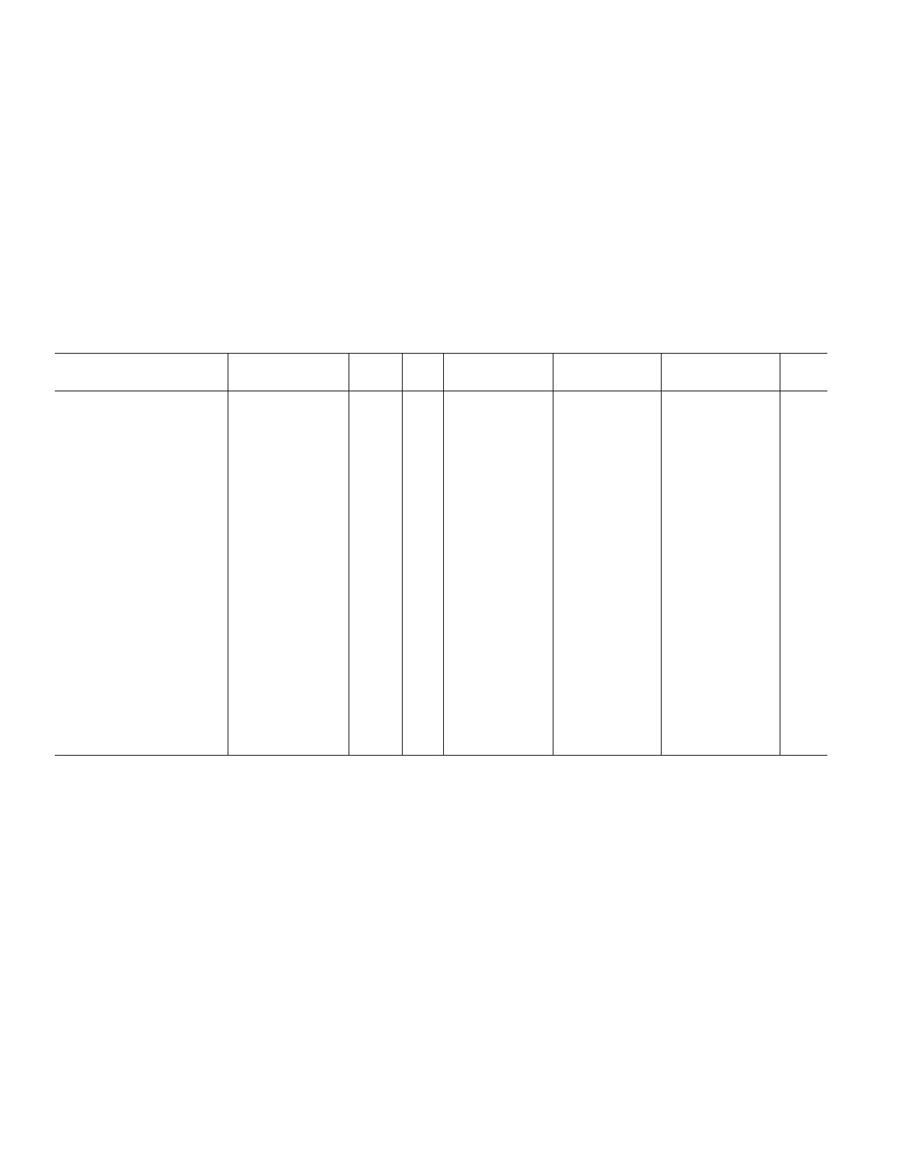
DC ELECTRICAL CHARACTERISTICS (Unless otherwise noted, AV = +3; ؎VS = ؎5 V; RF = 400 ⍀; RLOAD = 100 ⍀)
Parameter
Conditions
Input Offset Voltage1, 2
Input Offset Voltage TC2
Input Bias Current2
Inverting
Noninverting
Input Bias Current TC2
Noninverting
Inverting
Input Resistance
Noninverting
Input Capacitance
Noninverting
Common-Mode Input Range3
Common-Mode Rejection Ratio4
Power Supply Rejection Ratio
Open Loop Gain
TO
Nonlinearity
Output Voltage Range
Output Impedance
Output Current (50 Ω Load)
T = TMAX
T = TMIN to +25°C
T = TMIN to TMAX
T = TMIN to +25°C
∆VS = ± 5%
At DC
At DC
At DC
T = +25°C to TMAX
T = TMIN
NOTES
*Pending obsoletion: last-time buy October 25, 1999.
1Measured with respect to the inverting input.
2Typical is defined as the mean of the distribution.
3Measured in voltage follower configuration.
4Measured with VIN = +0.25 V.
Specifications subject to change without notice.
Test
Temp Level
+25°C I
Full IV
+25°C I
+25°C I
Full IV
Full IV
+25°C V
+25°C V
←
II
←
II
←
II
←
II
Full II
+25°C V
+25°C IV
+25°C II
+25°C V
←
II
←
II
AD9617JN/JR AD9617AQ/SQ* AD9617BQ/TQ*
Min Typ Max Min Typ Max Min Typ Max Units
–1.1 +0.5 +2.2 –1.1 +0.5 +2.2 +0.0 +0.5 +1.35 mV
–4 +3 +25 –4 +3 +25 –4 +3 +25 µV/°C
–50 0 +50 –50 0 +50 –25 0 +25 µA
–25 +5 +35 –25 +5 +35 –15 +5 +20 µA
–50 +30 +125 –50 +30 +125 –50 +30 +125 nA/°C
–50 +50 +150 –50 +50 +150 –50 +50 +150 nA/°C
60
60
60
kΩ
1.5
1.5
1.5
pF
± 1.4 ± 1.5
± 1.4 ± 1.5
± 1.4 ± 1.5
V
± 1.7 ± 1.8
± 1.7 ± 1.8
± 1.7 ± 1.8
V
44 48
44 48
44 48
dB
48 51
48 51
48 51
dB
48 51
48 51
48 51
dB
500
500
500
kΩ
10
10
10
ppm
± 3.4 ± 3.8
± 3.4 ± 3.8
± 3.4 +3.8
V
0.07
0.07
0.07
Ω
60
60
60
mA
50
50
50
mA
–2–
REV. B
Share Link: 