AD9552(RevC) Ver la hoja de datos (PDF) - Analog Devices
Número de pieza
componentes Descripción
Fabricante
AD9552 Datasheet PDF : 32 Pages
| |||
AD9552
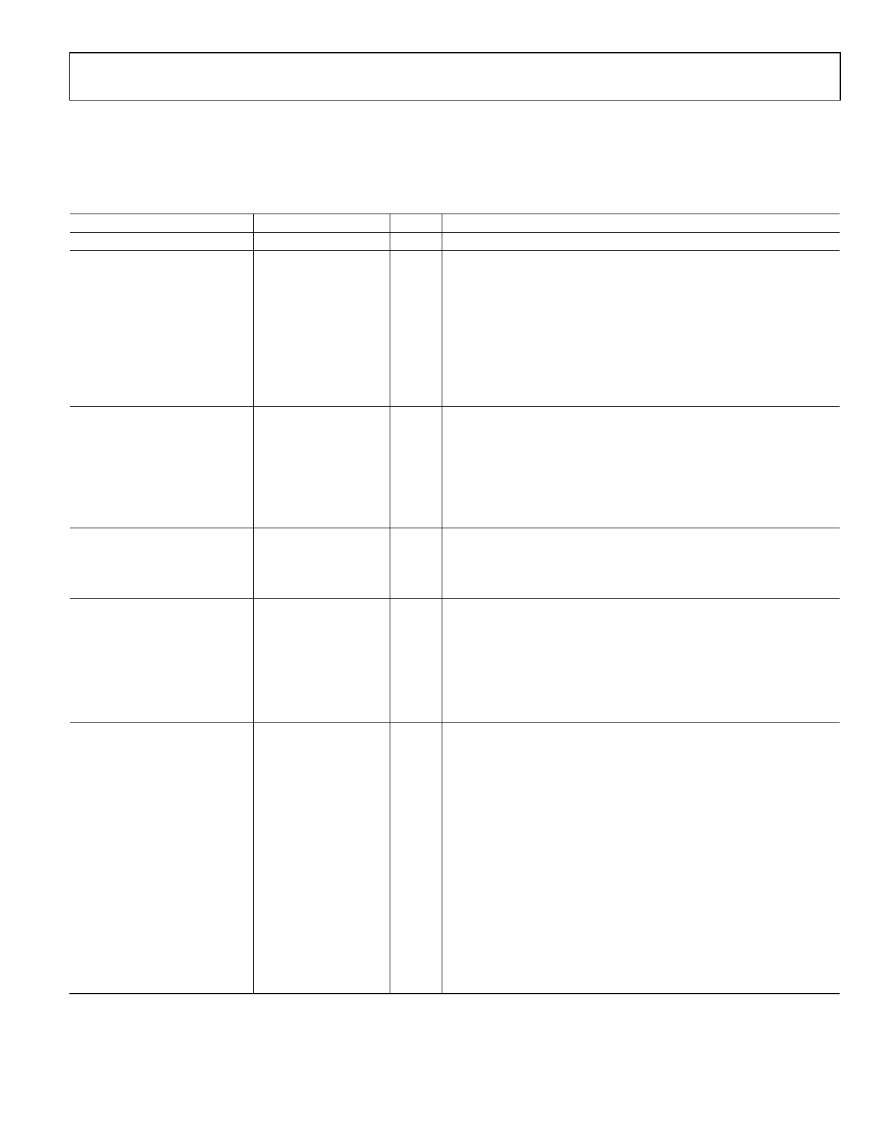
SPECIFICATIONS
Minimum (min) and maximum (max) values apply for the full range of supply voltage and operating temperature variations. Typical (typ)
values apply for VDD = 3.3 V; TA = 25°C, unless otherwise noted.
Table 1.
Parameter
SUPPLY VOLTAGE
POWER CONSUMPTION
Total Current
VDD Current By Pin
Pin 7
Pin 18
Pin 21
Pin 28
LVPECL Output Driver
Min Typ Max Unit
3.135 3.30 3.465 V
149 169 mA
2
3
mA
77 86 mA
35 41 mA
35 41 mA
36 41 mA
LOGIC INPUT PINS
INPUT CHARACTERISTICS1
Logic 1 Voltage, VIH
1.0
V
Logic 0 Voltage, VIL
Logic 1 Current, IIH
Logic 0 Current, IIL
LOGIC OUTPUT PINS
Output Characteristics
Output Voltage High, VOH 2.7
Output Voltage Low, VOL
RESET PIN
Input Characteristics2
Input Voltage High, VIH
1.8
Input Voltage Low, VIL
Input Current High, IINH
0.3
Input Current Low, IINL
31
Minimum Pulse Width High 2
REFERENCE CLOCK
INPUT CHARACTERISTICS
Frequency Range
7.94
6.57
0.8 V
3
μA
17 μA
V
0.4 V
V
1.3 V
12.5 μA
43 μA
ns
MHz
MHz
93.06 MHz
71.28 MHz
112.5 MHz
86.17 MHz
Test Conditions/Comments
Pin 7, Pin 18, Pin 21, Pin 28
At maximum output frequency with both output channels active
900 MHz with 100 Ω termination between both pins of the output
driver
For the CMOS inputs, a static Logic 1 results from either a pull-up
resistor or no connection
N3 = 255; 2× frequency multiplier enabled; valid for all VCO bands
N3 = 255; 2× frequency multiplier enabled; fVCO = 3.35 GHz, which con-
strains the frequency at OUT1 to be an integer sub-multiple of 3.35 GHz
(that is, fOUT1 = 3.35 ÷ M GHz, where M is the product of the P0 and P1
output divider values)
SDM4 disabled; N3 = 365; valid for all VCO bands
SDM4 enabled; N3 = 476; valid for all VCO bands
SDM4 disabled; N3 = 365; fVCO = 4.05 GHz, which constrains the
frequency at OUT1 to be an integer sub-multiple of 4.05 GHz (that is,
fOUT1 = 4.05÷M GHz, where M is the product of the P0 and P1 output
divider values)
SDM4 enabled; N3 = 476; fVCO = 4.05 GHz, which constrains the frequency
at OUT1 to be an integer sub-multiple of 4.05 GHz (that is, fOUT1 =
4.05÷M GHz, where M is the product of the P0 and P1 output divider
values)
Rev. C | Page 3 of 32
Share Link: 