AD9480(Rev0) Ver la hoja de datos (PDF) - Analog Devices
Número de pieza
componentes Descripción
Fabricante
AD9480 Datasheet PDF : 28 Pages
| |||
AD9480
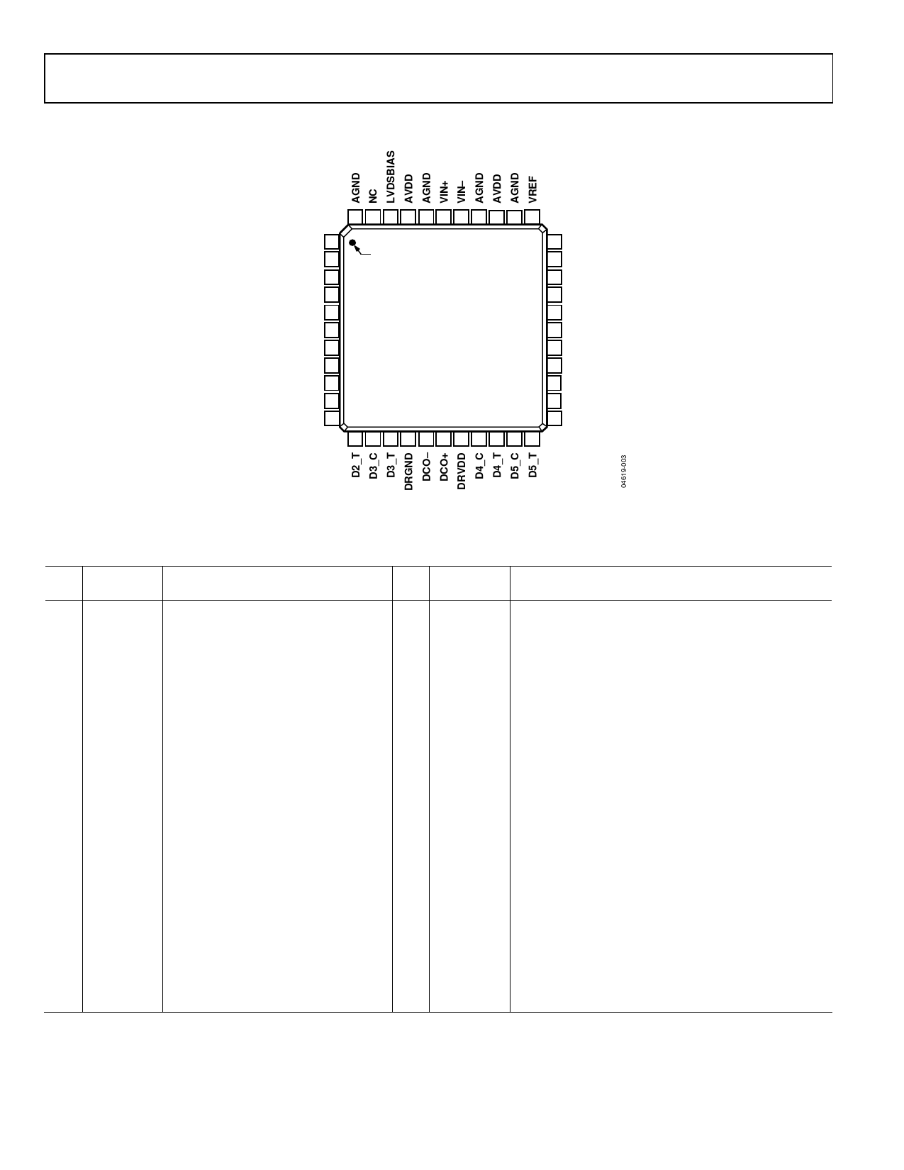
PIN CONFIGURATION AND FUNCTION DESCRIPTIONS
44 43 42 41 40 39 38 37 36 35 34
CLK+ 1
CLK– 2
AVDD 3
AGND 4
DRVDD 5
DRGND 6
D0_C (LSB) 7
D0_T (LSB) 8
D1_C 9
D1_T 10
D2_C 11
PIN 1
AD9480
TOP VIEW
(Not to Scale)
33 SENSE
32 AGND
31 AVDD
30 AGND
29 PDWN
28 S1
27 DRGND
26 D7_T (MSB)
25 D7_C (MSB)
24 D6_T
23 D6_C
NC = NO CONNECT 12 13 14 15 16 17 18 19 20 21 22
Table 7. Pin Function Descriptions
Pin No. Name Description
1
CLK+
Input Clock—True
2
CLK−
Input Clock—Complement
3
AVDD 3.3 V Analog Supply
4
AGND Analog Ground
5
DRVDD 3.3 V Digital Output Supply
6
DrGND Digital Ground
Figure 3. Pin Configuration
Pin No.
23
24
25
26
27
28
Name
D6_C
D6_T
D7_C
D7_T
DrGND
S1
7
D0_C
Data Ouput Bit 0—Complement (LSB) 29
8
D0_T
Data Output Bit 0—True (LSB)
30
9
D1_C
Data Output Bit 1—Complement
31
10
D1_T
Data Output Bit 1—True
32
11
D2_C
Data Output Bit 2—Complement
33
12
D2_T
Data Output Bit 2—True
34
13
D3_C
Data Output Bit 3—Complement
35
14
D3_T
Data Output Bit 3—True
36
15
DRGND Digital Ground
37
16
DCO− Data Clock Output—Complement
38
17
DCO+ Data Clock Output—True
39
18
DRVDD 3.3 V Digital Output Supply
40
19
D4_C
Data Output Bit 4—Complement
41
20
D4_T
Data Output Bit 4—True
42
21
D5_C
Data Output Bit 5—Complement
43
22
D5_T
Data Output Bit 5—True
44
PDWN
AGND
AVDD
AGND
SENSE
VREF
AGND
AVDD
AGND
VIN−
VIN+
AGND
AVDD
LVDSBIAS
AVDD
AGND
Description
Data Output Bit 6—Complement
Data Output Bit 6—True
Data Output Bit 7—Complement (MSB)
Data Output Bit 7—True (MSB)
Digital Ground
Data Format Select and Duty Cycle Stabilizer
Selection. See .
Power-Down Selection
Analog Ground
3.3 V Analog Supply
Analog Ground
Reference Mode Selection. See Table 9.
Voltage Reference Input/Output
Analog Ground
3.3 V Analog Supply
Analog Ground
Analog Input—Complement
Analog Input—True
Analog Ground
3.3 V Analog Supply
LVDS Output Current Adjust
3.3 V Analog Supply
Analog Ground
Rev. 0 | Page 8 of 28
Share Link: 