AD9393 Ver la hoja de datos (PDF) - Analog Devices
Número de pieza
componentes Descripción
Fabricante
AD9393 Datasheet PDF : 40 Pages
| |||
AD9393
One of the three input channels is represented in Figure 4.
In each processing channel, the three inputs are multiplied
by three separate coefficients marked a1, a2, and a3. These
coefficients are divided by 4096 to obtain nominal values
ranging from −0.9998 to +0.9998. The variable labeled a4 is
used as an offset control. The CSC_MODE setting is the same
for all three processing channels. This multiplies all coefficients
and offsets by a factor of 2 . CSC_MODE
audio, but also the sampling frequency (fS). The audio info-
frame also contains information about the N and CTS values
used to recreate the clock. With this information, it is possible
to regenerate the audio sampling frequency. The audio clock is
regenerated by dividing the 20-bit CTS value into the TMDS
clock, then multiplying by the 20-bit N value. This yields a
multiple of the sampling frequency of either 128 × fS or 256 ×
fS. It is possible for this to be specified up to 1024 × fS.
The functional diagram for a single channel of the CSC (as
shown in Figure 4) is repeated for the remaining G and B
channels. The coefficients for these channels are b1, b2, b3,
b4, c1, c2, c3, and c4.
a1[12:0]
a4[12:0]
CSC_MODE[1:0]
RIN[11:0]
×
×
1
4096
+
+
+
a2[12:0]
GIN[11:0]
×
×
1
4096
×4
2
ROUT[11:0]
×2
1
0
a3[12:0]
BIN[11:0]
×
×
1
4096
Figure 4. Single CSC Channel
A programming example and register settings for several
common conversions are listed in the Color Space Converter
(CSC) Common Settings section.
For a detailed functional description and more programming
examples that are compatible with the AD9393, refer to the
AN-795 Application Note, AD9880 Color Space Converter
User's Guide.
AUDIO PLL SETUP
Data contained in the audio infoframes (among other registers)
defines for the AD9393 HDMI receiver not only the type of
128 × fS
SOURCE DEVICE
DIVIDE
BY
N
CYCLE
TIME
COUNTER
CTS*
SINK DEVICE
VIDEO
CLOCK
N
REGISTER
N
TMDS
CLOCK
N*
÷ CTS
128 × fS
×N
*N AND CTS VALUES ARE TRANSMITTED USING THE
AUDIO CLOCK REGENERATION PACKET. VIDEO
CLOCK IS TRANSMITTED ON TMDS CLOCK CHANNEL.
Figure 5. N and CTS for Audio Clock
To provide the most flexibility in configuring the audio
sampling clock, an additional PLL is employed. The PLL
characteristics are determined by the loop filter design (see
Figure 6), the PLL charge pump current, and the VCO range
setting.
CP
CZ
PVDD
8nF
80nF
RZ
1.5kΩ
FILT
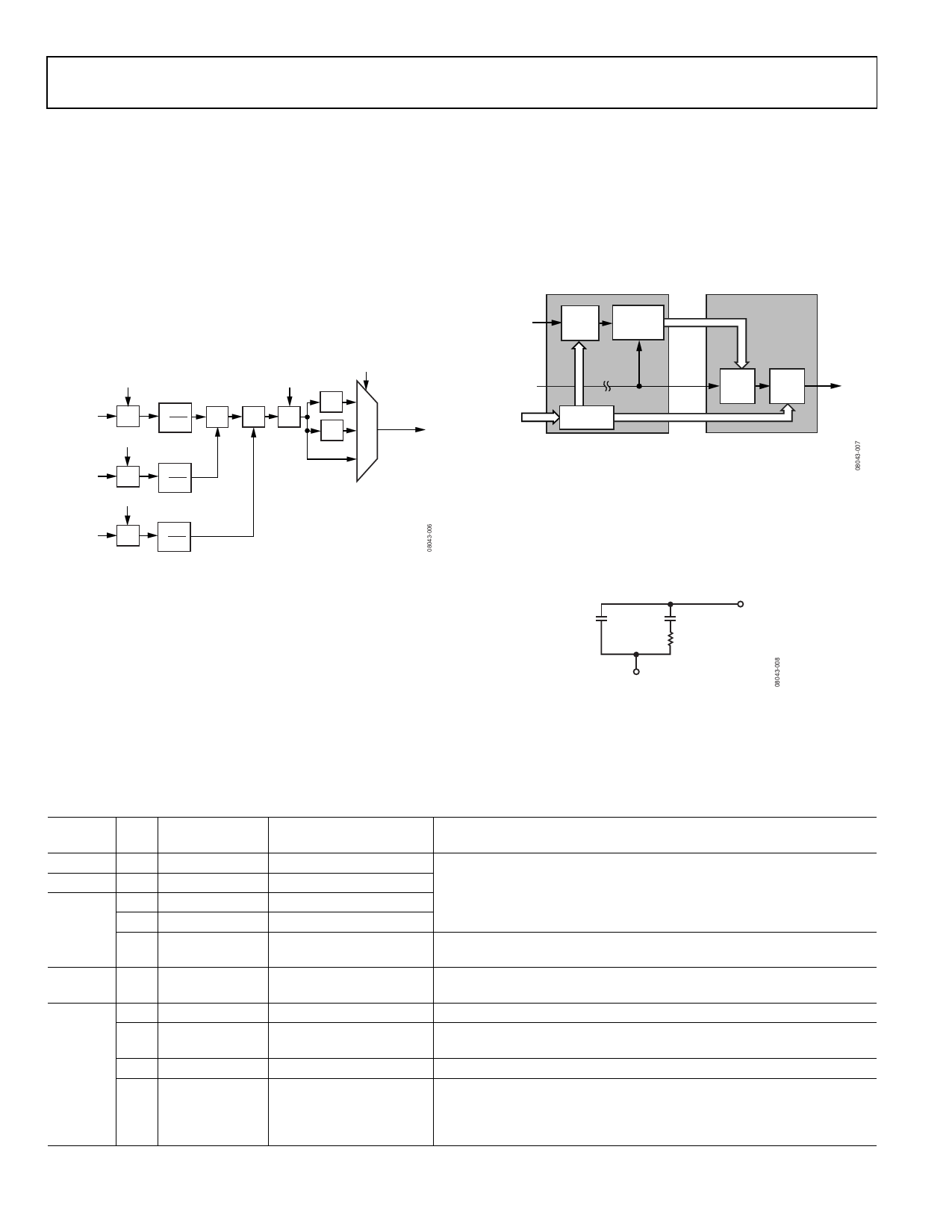
Figure 6. PLL Loop Filter Detail
To fully support all audio modes for all video resolutions up
to 1080i, it is necessary to adjust certain audio-related registers
from their power-on default values. Table 7 describes these
registers and gives the recommended settings.
Table 7. Audio Register Settings
Recommended
Register Bits Setting
0x01
[7:0] 0x00
0x02
[7:4] 0x40
0x03
[7:6] 01
[5:3] 010
[2] 1
Function
PLL divisor (MSBs)
PLL divisor (LSBs)
VCO range
Charge pump current
PLL enable
0x34
0x58
[5:4] 11
[7] 1
[6:4] 001
Audio frequency mode
override
MCLK PLL enable
MCLK PLL divisor
[3] 0
[2:0] 0**
N/CTS disable
MCLK sampling
frequency
Comments
The video PLL is used for the audio clock circuit when in HDMI mode. This
is done automatically.
In HDMI mode, this bit enables a lower frequency to be used for audio
MCLK generation.
Allows the chip to determine the low frequency mode of the audio PLL.
This enables the analog PLL to be used for audio MCLK generation.
When the analog PLL is enabled for MCLK generation, another frequency
divider is provided; these bits set the divisor to 2.
The N and CTS values should always be enabled.
000 = 128 × fS
001 = 256 × fS
010 = 384 × fS
011 = 512 × fS
Rev. 0 | Page 10 of 40
Share Link: 