AD9250 Ver la hoja de datos (PDF) - Analog Devices
Número de pieza
componentes Descripción
Fabricante
AD9250 Datasheet PDF : 45 Pages
| |||
AD9250
Data Sheet
TIMING SPECIFICATIONS
Table 5.
Parameter
SPI TIMING REQUIREMENTS (See Figure 62)
tDS
tDH
tCLK
tS
tH
tHIGH
tLOW
tEN_SDIO
tDIS_SDIO
tSPI_RST
Test Conditions/Comments
Setup time between the data and the rising edge of SCLK
Hold time between the data and the rising edge of SCLK
Period of the SCLK
Setup time between CS and SCLK
Hold time between CS and SCLK
Minimum period that SCLK should be in a logic high state
Minimum period that SCLK should be in a logic low state
Time required for the SDIO pin to switch from an input to an
output relative to the SCLK falling edge (not shown in figures)
Time required for the SDIO pin to switch from an output to an
input relative to the SCLK rising edge (not shown in figures)
Time required after hard or soft reset until SPI access is available
(not shown in figures)
Min Typ Max Unit
2
ns
2
ns
40
ns
2
ns
2
ns
10
ns
10
ns
10
ns
10
ns
500
µs
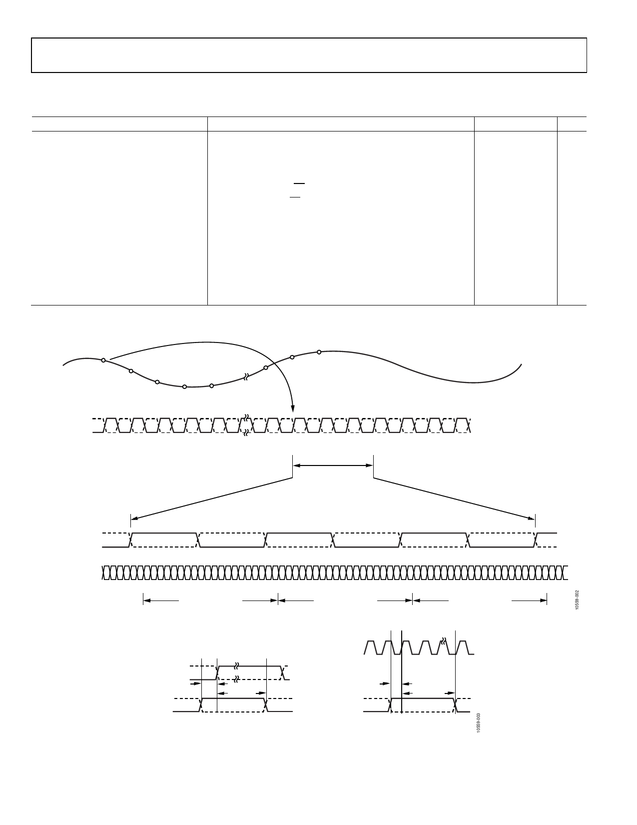
Timing Diagrams
ANALOG
INPUT
SIGNAL
N – 36
N – 35
N – 34
N – 33
SAMPLE N
N+1
N–1
CLK–
CLK+
CLK–
CLK+
SERDOUT1±
SERDOUT0±
SAMPLE N – 36
ENCODED INTO 2
8b/10b SYMBOLS
SAMPLE N – 35
ENCODED INTO 2
8b/10b SYMBOLS
Figure 2. Data Output Timing
RFCLK
CLK+
CLK– tREFS
SYSREF+
tREFH
tREFSRF
SYSREF+
SYSREF–
SYSREF–
NOTES
1. CLOCK INPUT IS EITHER RFCLK OR CLK±, NOT BOTH.
Figure 3. SYSREF± Setup and Hold Timing
Rev. E | Page 10 of 45
SAMPLE N – 34
ENCODED INTO 2
8b/10b SYMBOLS
tREFHRF
Share Link: 