AD827A(RevB) Ver la hoja de datos (PDF) - Analog Devices
Número de pieza
componentes Descripción
Fabricante
AD827A Datasheet PDF : 8 Pages
| |||
AD827
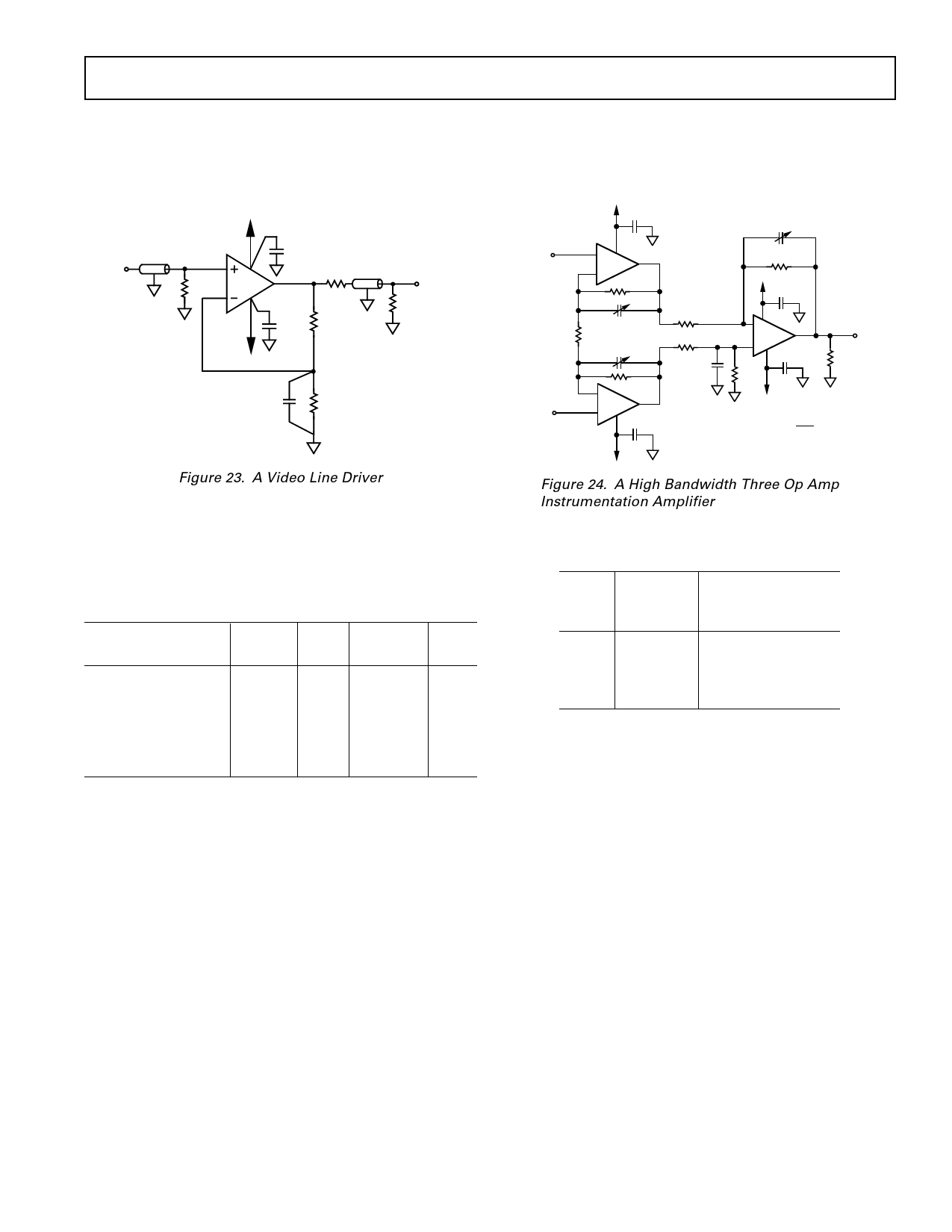
VIDEO LINE DRIVER
The AD827 functions very well as a low cost, high speed line
driver for either terminated or unterminated cables. Figure 23
shows the AD827 driving a doubly terminated cable in a
follower configuration.
Figure 23. A Video Line Driver
The termination resistor, RT, (when equal to the cable’s
characteristic impedance) minimizes reflections from the far end
of the cable. While operating from ±5 V supplies, the AD827
maintains a typical slew rate of 200 V/µs, which means it can
drive a ±1 V, 30 MHz signal into a terminated cable.
Table I. Video Line Driver Performance Summary
VIN*
VSUPPLY
0 dB or ±500 mV Step ±15
0 dB or ±500 mV Step ±15
0 dB or ±500 mV Step ±15
0 dB or ±500 mV Step ±5
0 dB or ±500 mV Step ±5
0 dB or ±500 mV Step ±5
CC
20 pF
15 pF
0 pF
20 pF
15 pF
0 pF
–3 dB BW
23 MHz
21 MHz
13 MHz
18 MHz
16 MHz
11 MHz
Over-
shoot
4%
0%
0%
2%
0%
0%
NOTE
*–3 dB bandwidth numbers are for the 0 dBm signal input. Overshoot numbers
are the percent overshoot of the 1 Volt step input.
A back-termination resistor (RBT, also equal to the characteristic
impedance of the cable) may be placed between the AD827
output and the cable input, in order to damp any reflected
signals caused by a mismatch between RT and the cable’s
characteristic impedance. This will result in a flatter frequency
response, although this requires that the op amp supply ±2 V to
the output in order to achieve a ±1 V swing at resistor RT.
A HIGH SPEED 3 OP AMP INSTRUMENTATION
AMPLIFIER CIRCUIT
The instrumentation amplifier circuit shown in Figure 24 can
provide a range of gains. The chart of Table II details
performance.
+VS
0.1µF
–VIN
3 + 1/2 8 1
2 AD827
–
1kΩ
TRIM FOR
RG
OPTIMUM
BANDWIDTH
7 – 15 pF
6 – 1kΩ
1/2
7
+VIN
5
AD827
+4
0.1µF
TRIM FOR BEST
SETTLING TIME
2 – 8pF
2kΩ
2kΩ
3pF
2kΩ
+VS
0.1µF
27
–
6
AD847
3+
4 0.1µF
2kΩ
VOUT
2kΩ
RL
–VS
CIRCUIT GAIN = 2000 + 1
RG
–VS
NOTE: PINOUT SHOWN IS FOR MINIDIP PACKAGE
Figure 24. A High Bandwidth Three Op Amp
Instrumentation Amplifier
Table II. Performance Specifications for the
Three Op Amp Instrumentation Amplifier
Gain
1
2
10
100
RG
Open
2k
226 Ω
20 Ω
Small Signal
Bandwidth
@ 1 V p-p Output
16.1 MHz
14.7 MHz
4.9 MHz
660 kHz
A TWO-CHIP VOLTAGE-CONTROLLED AMPLIFIER
(VCA) WITH EXPONENTIAL RESPONSE
Voltage-controlled amplifiers are often used as building blocks
in automatic gain control systems. Figure 25 shows a two-chip
VCA built using the AD827 and the AD539, a dual, current-
output multiplier. As configured, the circuit has its two
INPUT RANGE:
10MV TO 3V (55dB)
AD539
VX 1 CONTROL W1 16
2
15
VIN
HF COMP
0.01µF 3 CH 1
Z1
CH1 14
IN
+5V
4.7Ω
4
0.1µF
+VS
–5V 4.7Ω
5 –VS
0.1µF
6 CH2
IN
7 INPUT
COM
OUT
13
BASE
COM 12
CH2 11
OUT 10
Z2
8 OUTPUT
COM
9
W2
2pF
C3
2pF
C4
*PINOUT SHOWN IS FOR MINI-DIP PACKAGE
VOUT AT TERMINATION RESISTOR, RT
=
VX2 VIN
8V2
VOUT AT PIN & OF AD827 =
VX2 VIN
4V2
+5V
0.1µF
2– 8
1/2
3
AD827
+*
1
5+
1/2
*
7
6
AD827
–4
0.1µF
COAX LINE OUTPUT
50Ω
RT 50Ω
–5V
Figure 25. A Wide Range Voltage-Controlled
Amplifier Circuit
Share Link: 