AD795JN Ver la hoja de datos (PDF) - Analog Devices
Número de pieza
componentes Descripción
Fabricante
AD795JN Datasheet PDF : 16 Pages
| |||
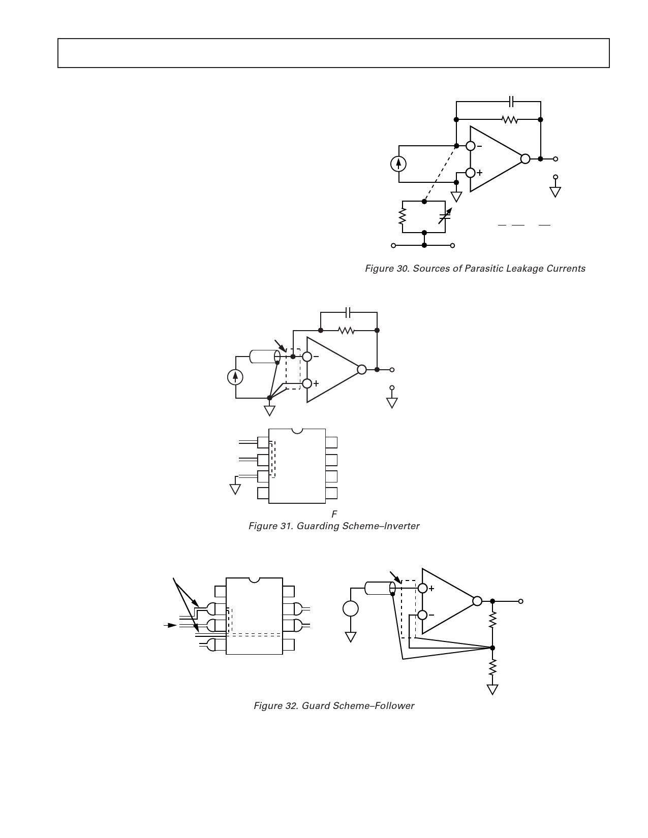
CIRCUIT BOARD NOTES
The AD795 is designed for mounting on PC boards. Maintaining
picoampere resolution in those environments requires a lot of
care. Both the board and the amplifier’s package have finite
resistance. Voltage differences between the input pins and other
pins as well as PC board metal traces will cause parasitic currents
(Figure 30) larger than the AD795’s input current unless special
precautions are taken. Two methods of minimizing parasitic
leakages are guarding of the input lines and maintaining adequate
insulation resistance.
Figures 31 and 32 show the recommended guarding schemes
for follower and inverted topologies. Pin 1 is not connected, and
can be safely connected to the guard. The high impedance input
trace should be guarded on both edges for its entire length.
AD795
IS
IP
RP
VS
CF
RF
VE
2
AD795 6
3
+
VOUT
–
CP
IP
=
VS
RP
+
dCP
dT
VS+ddVTS
CP
Figure 30. Sources of Parasitic Leakage Currents
GUARD
IS
CF
RF
2
AD795 6
3
+
VOUT
–
1
8
2
7
3
TOP VIEW
6
4 ("R" PACKAGE) 5
NOTE:
ON THE "R" PACKAGE
PINS 1, 5 AND 8 ARE OPEN
AND CAN BE CONNECTED
TO ANALOG COMMON OR
TO THE DRIVEN GUARD TO
REDUCE LEAKAGE.
F
Figure 31. Guarding Scheme–lnverter
GUARD TRACES
GUARD
INPUT
TRACE
1
8
AD795
2
TOP VIEW
7
3
6
+
VS
–
–VS
4
5
CONNECT TO JUNCTION
OF RF AND RI, OR TO PIN 6
FOR UNITY GAIN.
3
AD795 6
2
Figure 32. Guard Scheme–Follower
+
VOUT
RF
RI
–
REV. B
–9–
Share Link: 