MXED102 Ver la hoja de datos (PDF) - Clare Inc => IXYS
Número de pieza
componentes Descripción
Fabricante
MXED102 Datasheet PDF : 20 Pages
| |||
Preliminary
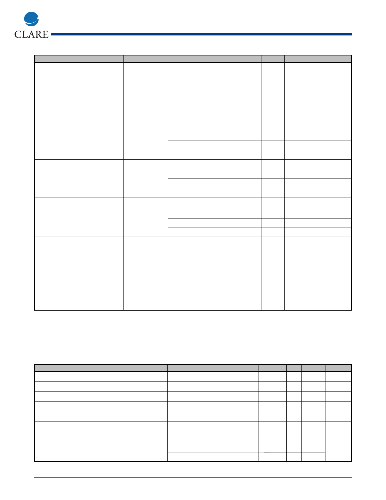
MXED102
Output Current Channels:
Parameter
Channel output impedance
during precharge
Channel output charging
current during precharge
Driver output current source
current and current error
Sym
-
-
IOUT
Single die, per bank driver
output current source matching
-
Die to die, per bank average
driver output current source
-
matching
Exposure clock rising edge to
-
output going high/low
Channel output current rise/fall
-
time
Shorting switch on resistance
-
to ISHRT pin
Shorting switch discharge
-
current to ISHRT pin
Operating Condition
5 < VPRE < VDD-4,
VPRE - VIOUT < 4 V
5 < VPRE < VDD-4,
VPRE - VIOUT > 4 V
IOUT = -4 uA x 1.2 ** N
for N = reg value,
0 < N < 32,
0 < VIOUT < VDD-3
-20 uA < IIOUT < -75 uA
-75 uA < IIOUT < -1 mA
0 < VIOUT < VDD-3,
VIOUT mismatch < 2 V
-20 uA < IIOUT < -75 uA
-75 uA < IIOUT < -1 mA
0 < VIOUT < VDD-3,
VOUT mismatch < 2 V
20 uA < IIOUT < 150 uA
-150 uA < IIOUT < -1 mA
Delay to 50% point
10% to 90%
VIOUT < 8 V
VIOUT > 8 V
Min Typ Max Unit
-
- 2000 ohms
-2.3 -
-
mA
-
-
-
-
-3
- +3 uA
-4
- +4
%
-
-
-
-
-1.5 - +1.5 uA
-2
- +2
%
-
-
-
-
-1.5 - 1.5 uA
-1
-
1
%
-
- 220 nS
-
- 250 nS
-
- 400 ohms
25
-
-
mA
Chip Monitor Analog to Digital Converter:
The ADC is intended to be used to calibrate the precharge circuit. The ADC on the column driver chip designated
as the master can be monitored by the controller. Which parameter the ADC is monitoring is determined by the A/D
Converter Control Register. Results can be monitored on the A/D Converter Output Register.
Parameter
Bits
Linearity
Accuracy
Output for low voltage input
Sym
-
-
-
-
Output for high voltage input
-
Conversion time in CLKEX counts -
Operating Condition
-
-
-
Vout(8 bit word) =
255 * Vin / 5.0
Vout(8 bit word) =
255 * Vin / 30.0
Control reg 2, bit 1 = 0
Control reg 2, bit 1 = 1
Min Typ Max Unit
-8
-
-
- .5 LSB - .5 LSB -
- 1 LSB - 1 LSB -
-
-
-
-
-
-
-
-
896 -
112 -
- CLKEX
- counts
Rev. 2
www.clare.com
9
Share Link: 