AD745KRZ-16 Ver la hoja de datos (PDF) - Analog Devices
Número de pieza
componentes Descripción
Fabricante
AD745KRZ-16 Datasheet PDF : 12 Pages
| |||
AD745
HOW CHIP PACKAGE TYPE AND POWER DISSIPATION
AFFECT INPUT BIAS CURRENT
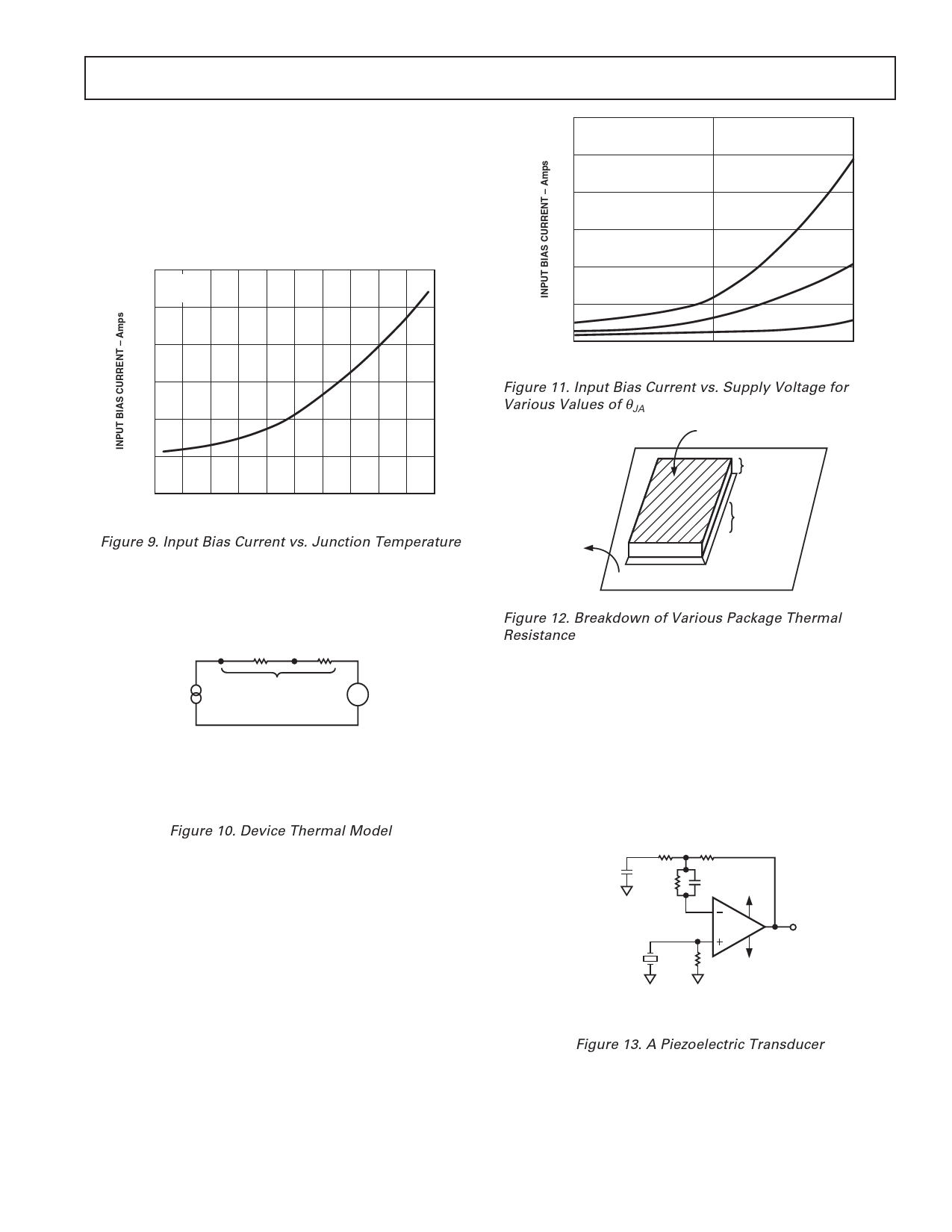
As with all JFET input amplifiers, the input bias current of the
AD745 is a direct function of device junction temperature, IB
approximately doubling every 10°C. Figure 9 shows the rela-
tionship between bias current and junction temperature for the
AD745. This graph shows that lowering the junction tempera-
ture will dramatically improve IB.
10–6
10–7
VS = 15V
TA = 25؇C
10–8
10–9
10–10
10–11
10–12
–60 –40 –20 0
20 40 60 80 100 120 140
JUNCTION TEMPERATURE – ؇C
Figure 9. Input Bias Current vs. Junction Temperature
The dc thermal properties of an IC can be closely approximated
by using the simple model of Figure 10 where current represents
power dissipation, voltage represents temperature, and resistors
represent thermal resistance (θ in °C/watt).
TJ
JC
CA
JA
PIN
TA
WHERE:
PIN = DEVICE DISSIPATION
TA = AMBIENT TEMPERATURE
TJ = JUNCTION TEMPERATURE
JC = THERMAL RESISTANCE – JUNCTION TO CASE
CA = THERMAL RESISTANCE – CASE TO AMBIENT
Figure 10. Device Thermal Model
From this model TJ = TA+θJA PIN. Therefore, IB can be deter-
mined in a particular application by using Figure 9 together with
the published data for θJA and power dissipation. The user can
modify θJA by use of an appropriate clip-on heat sink such as the
Aavid #5801. Figure 11 shows bias current versus supply voltage
with θJA as the third variable. This graph can be used to predict
bias current after θJA has been computed. Again bias current will
double for every 10°C.
300
TA = 25؇C
200
JA = 165؇C/W
100
JA = 115؇C/W
JA = 0؇C/W
0
5
10
15
SUPPLY VOLTAGE – ؎Volts
Figure 11. Input Bias Current vs. Supply Voltage for
Various Values of θJA
TJ
TA
CASE
A
(J TO DIE
MOUNT)
B
(DIE MOUNT
TO CASE)
A + B = JC
Figure 12. Breakdown of Various Package Thermal
Resistance
REDUCED POWER SUPPLY OPERATION FOR
LOWER IB
Reduced power supply operation lowers IB in two ways: first, by
lowering both the total power dissipation and, second, by reduc-
ing the basic gate-to-junction leakage (Figure 11). Figure 13
shows a 40 dB gain piezoelectric transducer amplifier, which
operates without an ac coupling capacitor, over the –40°C to
+85°C temperature range. If the optional coupling capacitor,
C1, is used, this circuit will operate over the entire –55°C to
+125°C temperature range.
100⍀ 10k⍀
C1*
108⍀**
CT**
+5V
TRANSDUCER
CT
108⍀
AD745
–5V
*OPTIONAL DC BLOCKING CAPACITOR
**OPTIONAL, SEE TEXT
Figure 13. A Piezoelectric Transducer
REV. D
–9–
Share Link: 