AD7280A Ver la hoja de datos (PDF) - Analog Devices
Número de pieza
componentes Descripción
Fabricante
AD7280A Datasheet PDF : 48 Pages
| |||
AD7280A
TIMING SPECIFICATIONS
VDD = 8 V to 30 V, VSS = 0 V, DVCC = AVCC = VREG, VDRIVE = 2.7 V to 5.5 V, TA = −40°C to +105°C, unless otherwise noted.
Table 3.
Parameter1
tCONV
tACQ
tACQ
tACQ
tACQ
tDELAY
tWAIT
fSCLK
tQUIET
t1 2
t2
t3
t4
t5
t6 3
t7
t8
t9
t10 4
t11
t12
Min
425
425
340
340
665
665
1005
1005
1340
1340
5
Typ
560
400
800
1200
1600
200
200
0.4
10
5
4
20
0.45 × tSCLK
0.45 × tSCLK
100
3
Max
695
720
465
470
1010
1030
1460
1510
1890
1945
250
1
50
20
28
10
Unit
Description
ADC conversion time
ns
−40°C to +85°C
ns
−40°C to +105°C
ADC acquisition time, Bits[D6:D5] of the control register set to 00
ns
−40°C to +85°C
ns
−40°C to +105°C
ADC acquisition time, Bits[D6:D5] of the control register set to 01
ns
−40°C to +85°C
ns
−40°C to +105°C
ADC acquisition time, Bits[D6:D5] of the control register set to 10
ns
−40°C to +85°C
ns
−40°C to +105°C
ADC acquisition time, Bits[D6:D5] of the control register set to 11
ns
−40°C to +85°C
ns
−40°C to +105°C
ns
Propagation delay between the falling edges of CNVST of adjacent
parts in the daisy chain
μs
Time required between the end of conversions and the beginning
of readback of the conversion results
MHz
Frequency of serial read clock
ns
Minimum quiet time required between the end of a serial read and
the start of the next conversion
μs
CNVST low pulse
ns
CS falling edge to SCLK rising edge
ns
Delay from CS falling edge until SDO is three-state disabled
ns
SDI setup time prior to SCLK falling edge
ns
SDI hold time after SCLK falling edge
ns
Data access time after SCLK rising edge
ns
SCLK to data valid hold time
ns
SCLK high pulse width
ns
SCLK low pulse width
ns
CS rising edge to SCLK rising edge
ns
CS rising edge to SDO high impedance
μs
CS high time required between each 32-bit write/read command
1 Sample tested during initial release to ensure compliance. All input signals are specified with tR = tF = 5 ns (10% to 90% of VDRIVE) and timed from a voltage level of 1.6 V.
All timing specifications given are with a 25 pF load capacitance.
2 Maximum allowed CNVST low pulse time to ensure that a software power-down state is not entered when the CNVST pin is not gated.
3 Time required for the output to cross 0.4 V or 2.4 V.
4 t10 applies when using a continuous SCLK. Guaranteed by design.
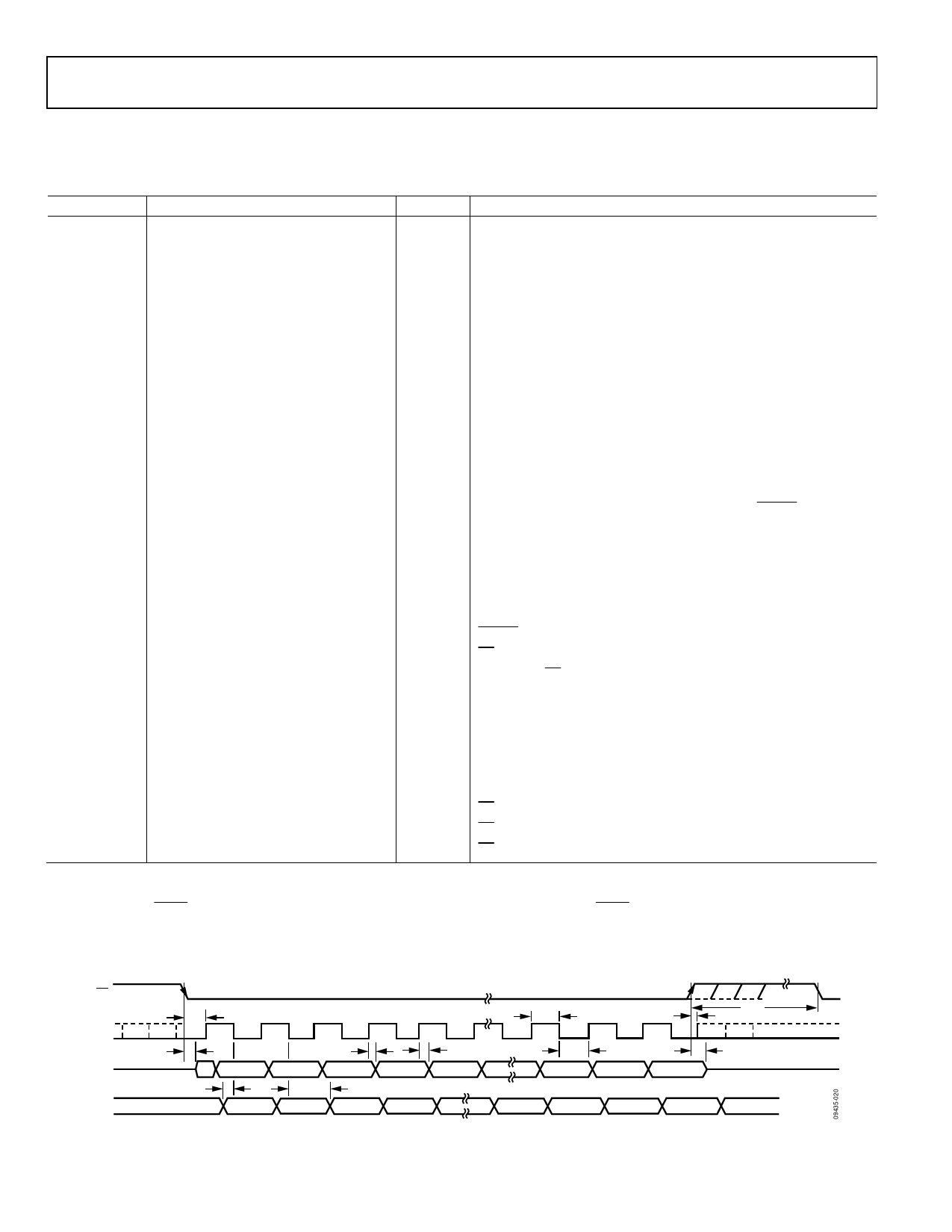
Timing Diagram
CS
SCLK
t2
1
2
3
4
t3
t6
t7
SDO
SDI
THREE-STATE
t4
MSB
MSB
MSB – 1
t5
MSB – 1
t8
t9
Figure 2. Serial Interface Timing Diagram
t10
32
t11
LSB
LSB
t12
THREE-STATE
Rev. 0 | Page 6 of 48
Share Link: 