AD6657A Ver la hoja de datos (PDF) - Analog Devices
Número de pieza
componentes Descripción
Fabricante
AD6657A Datasheet PDF : 36 Pages
| |||
AD6657A
Data Sheet
TIMING SPECIFICATIONS
AVDD = 1.8 V, DRVDD = 1.8 V, fS = 185 MSPS, 1.75 V p-p differential input, VIN = −1.0 dBFS differential input, and default SPI, unless
otherwise noted.
Table 5.
Parameter
Description
Min
Typ
Max Unit
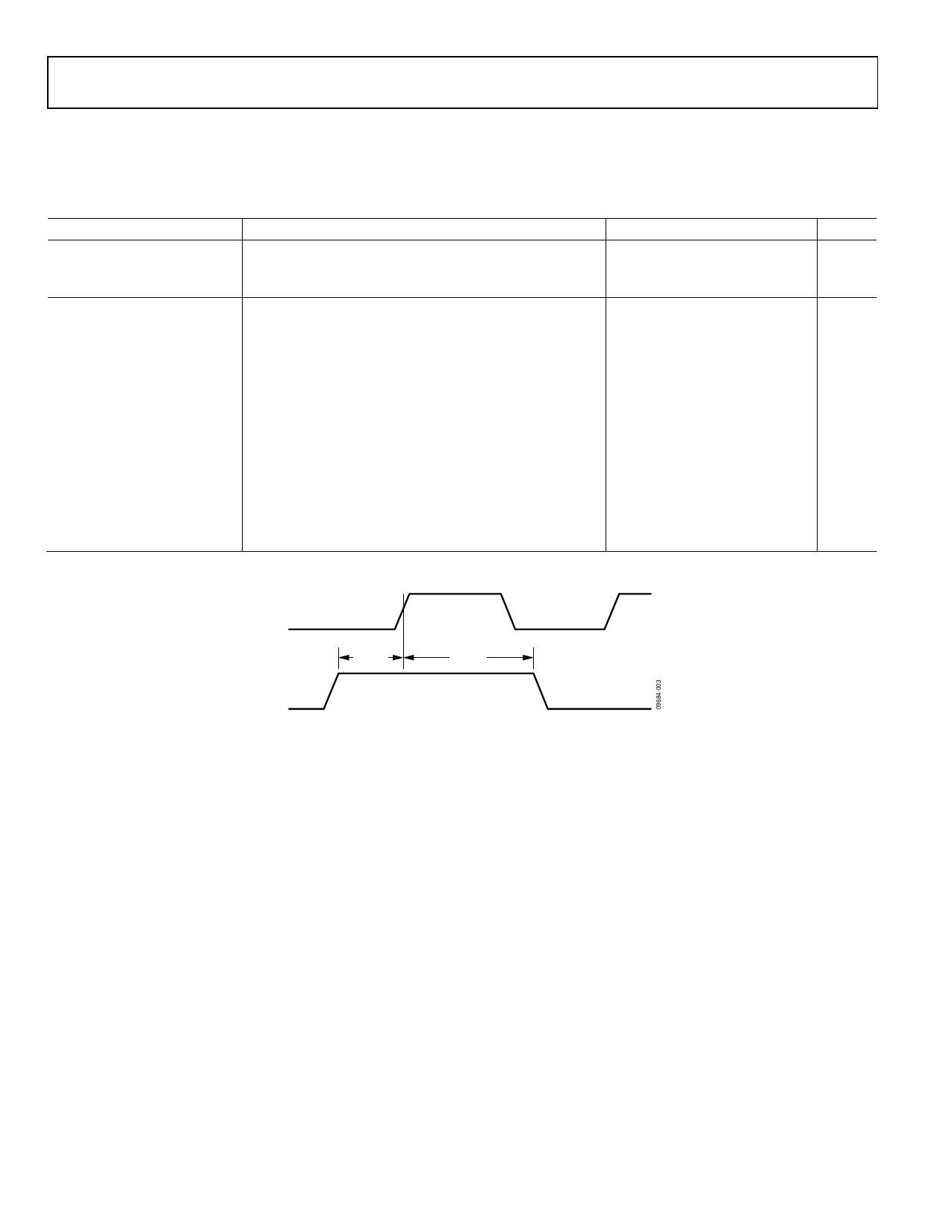
SYNC TIMING REQUIREMENTS See Figure 3 for details
tSSYNC
tHSYNC
SYNC to rising edge of CLK setup time
SYNC to rising edge of CLK hold time
0.24
ns
0.40
ns
SPI TIMING REQUIREMENTS
See Figure 60 for details, except where noted
tDS
Setup time between the data and the rising edge of SCLK 2
ns
tDH
Hold time between the data and the rising edge of SCLK
2
ns
tCLK
Period of the SCLK
40
ns
tS
Setup time between CSB and SCLK
2
ns
tH
Hold time between CSB and SCLK
2
ns
tHIGH
SCLK pulse width high
10
ns
tLOW
SCLK pulse width low
10
ns
tEN_SDIO
Time required for the SDIO pin to switch from an input to 10
ns
an output relative to the SCLK falling edge (not pictured in
Figure 60)
tDIS_SDIO
Time required for the SDIO pin to switch from an output to 10
ns
an input relative to the SCLK rising edge (not pictured in
Figure 60)
Sync Input Timing Diagram
CLK+
SYNC
tSSYNC
tHSYNC
Figure 3. SYNC Input Timing Requirements
Rev. A | Page 10 of 36
Share Link: 