AD600 Ver la hoja de datos (PDF) - Analog Devices
Número de pieza
componentes Descripción
Fabricante
AD600 Datasheet PDF : 32 Pages
| |||
AD600/AD602
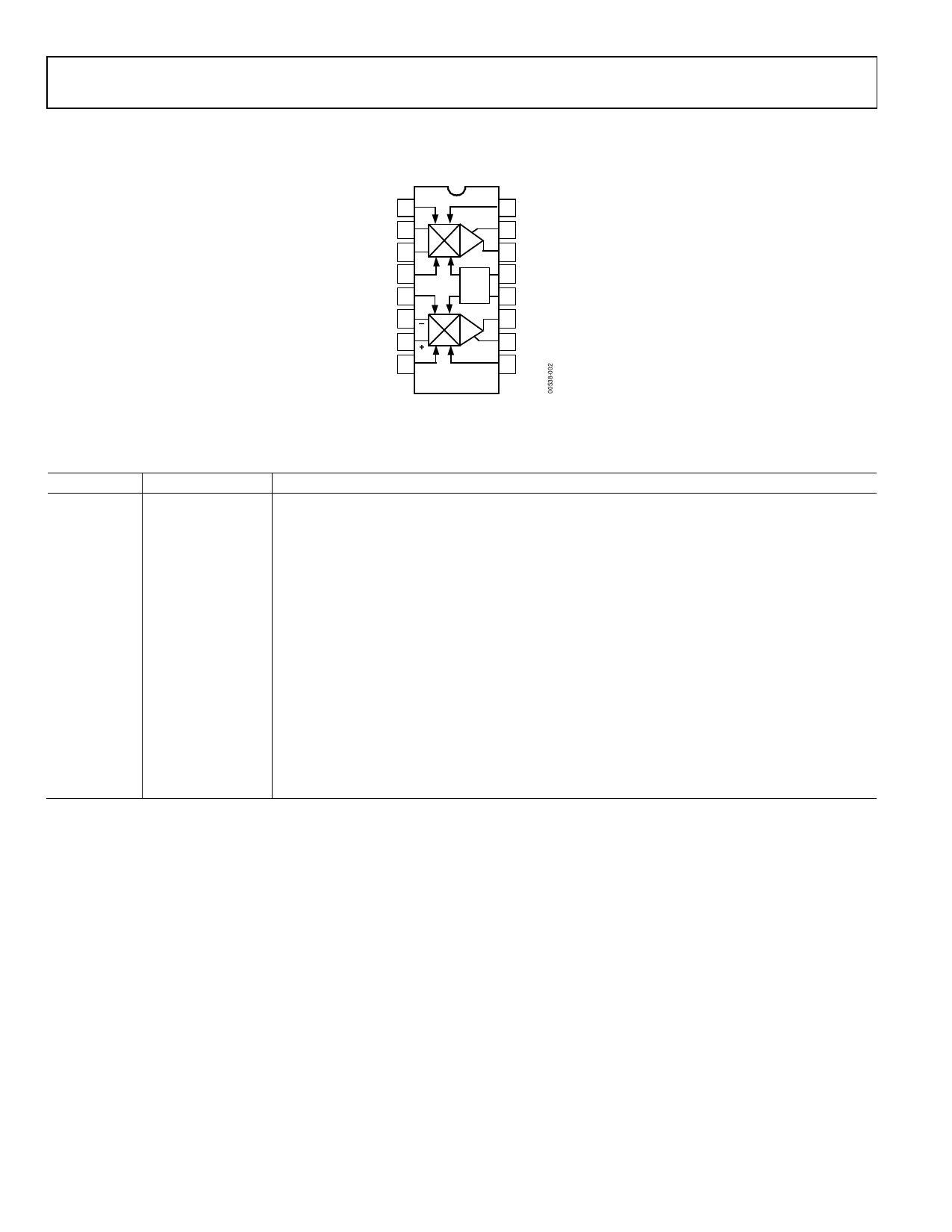
PIN CONFIGURATION AND FUNCTION DESCRIPTIONS
C1LO 1
16 C1HI
A1HI 2 +
A1LO 3 –
GAT1 4
GAT2 5
A1
REF
15 A1CM
14 A1OP
13 VPOS
12 VNEG
A2LO 6 –
A2HI 7 +
11 A2OP
A2
10 A2CM
C2LO 8
AD600 /
AD602
9 C2HI
Figure 2. Pin Configuration
Table 3. Pin Function Descriptions
Pin No.
Mnemonic
Description
1
C1LO
CH1 Gain-Control Input Low. Positive voltage reduces CH1 gain.
2
A1HI
CH1 Signal Input High. Positive voltage increases CH1 output.
3
A1LO
CH1 Signal Input Low. Usually connected to CH1 input ground.
4
GAT1
CH1 Gating Input. A logic high shuts off the CH1 signal path.
5
GAT2
CH2 Gating Input. A logic high shuts off the CH2 signal path.
6
A2LO
CH2 Signal Input Low. Usually connected to CH2 input ground.
7
A2HI
CH2 Signal Input High. Positive voltage increases CH2 output.
8
C2LO
CH2 Gain-Control Input Low. Positive voltage reduces CH2 gain.
9
C2HI
CH2 Gain-Control Input High. Positive voltage increases CH2 gain.
10
A2CM
CH2 Common. Usually connected to CH2 output ground.
11
A2OP
CH2 Output.
12
VNEG
Negative Supply for Both Amplifiers.
13
VPOS
Positive Supply for Both Amplifiers.
14
A1OP
CH1 Output.
15
A1CM
CH1 Common. Usually connected to CH1 output ground.
16
C1HI
CH1 Gain-Control Input High. Positive voltage increases CH1 gain.
Rev. F | Page 6 of 32
Share Link: 