AD5539 Ver la hoja de datos (PDF) - Analog Devices
Número de pieza
componentes Descripción
Fabricante
AD5539 Datasheet PDF : 16 Pages
| |||
AD5539
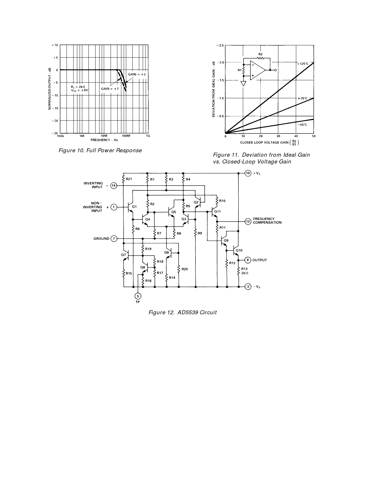
Figure 10. Full Power Response
Figure 11. Deviation from Ideal Gain
vs. Closed-Loop Voltage Gain
Figure 12. AD5539 Circuit
FUNCTIONAL DESCRIPTION
The AD5539 is a two-stage, very high frequency amplifier.
Darlington input transistors Q1, Q4–Q2, Q3 form the first
stage—a differential gain amplifier with a voltage gain of ap-
proximately 50. The second stage, Q5, is a single-ended ampli-
fier whose input is derived from one phase of the differential
amplifier output; the other phase of the differential output is
then summed with the output of Q5. The all NPN design of the
AD5539 is configured such that the emitter of Q5 is returned,
via a small resistor to ground; this eliminates the need for sepa-
rate level shifting circuitry.
The output stage, consisting of transistors Q9 and Q10, is a
Darlington voltage follower with a resistive pull-down. The bias
section, consisting of transistors Q6, Q7 and Q8, provides a
stable emitter current for the input section, compensating for
temperature and power supply variations.
SOME GENERAL PRINCIPLES OF HIGH FREQUENCY
CIRCUIT DESIGN
In designing practical circuits with the AD5539, the user must
remember that whenever very high frequencies are involved,
some special precautions are in order. All real-world applica-
tions circuits must be built using proper RF techniques: the use
of short interconnect leads, adequate shielding, groundplanes,
and very low profile IC sockets. In addition, very careful bypass-
ing of power supply leads is a must.
Low-impedance transmission line is frequently used to carry sig-
nals at RF frequencies: 50 Ω line for telecommunications pur-
poses and 75 Ω for video applications. The AD5539 offers a
relatively low output impedance; therefore, some consideration
must be given to impedance matching. A common matching
technique involves simply placing a resistor in series with the
amplifier output that is equal to the characteristic impedance of
the transmission line. This provides a good match (although at a
loss of 6 dB), adequate for many applications.
All of the circuits here were built and tested in a 50 Ω system.
Care should be taken in adapting these circuits for each particu-
lar use. Any system which has been properly matched and ter-
minated in its characteristic impedance should have the same
small signal frequency response as those shown in this
data sheet.
–6–
REV. B
Share Link: 