AD5539SQ/883B Ver la hoja de datos (PDF) - Analog Devices
Número de pieza
componentes Descripción
Fabricante
AD5539SQ/883B Datasheet PDF : 16 Pages
| |||
AD5539
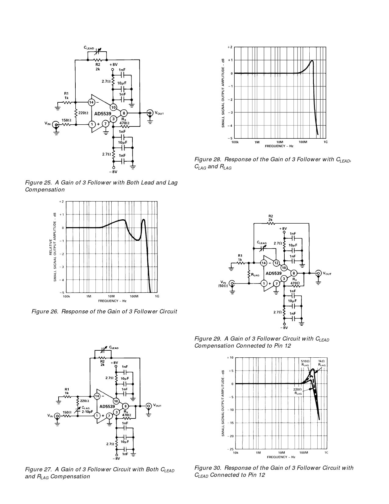
Figure 25. A Gain of 3 Follower with Both Lead and Lag
Compensation
Figure 28. Response of the Gain of 3 Follower with CLEAD,
CLAG and RLAG
These same principles may be applied when capacitor CLEAD is
connected to Pin 12 (Figure 29). Figure 30 shows the band-
width of the gain of 3 amplifier for various values of RLAG. It can
be seen from these response plots that a high noise gain is still
needed to achieve a reasonably flat response (the smaller the
Figure 26. Response of the Gain of 3 Follower Circuit
Adding a lag capacitor (Figure 27) will greatly reduce the
midband and low frequency noise gain of the circuit while sacri-
ficing only a small amount of bandwidth as shown in Figure 28.
Figure 29. A Gain of 3 Follower Circuit with CLEAD
Compensation Connected to Pin 12
Figure 27. A Gain of 3 Follower Circuit with Both CLEAD
and RLAG Compensation
Figure 30. Response of the Gain of 3 Follower Circuit with
CLEAD Connected to Pin 12
–10–
REV. B
Share Link: 