AD1990 Ver la hoja de datos (PDF) - Analog Devices
Número de pieza
componentes Descripción
Fabricante
AD1990 Datasheet PDF : 16 Pages
| |||
Preliminary Technical Data
Programmable Gain Amplifier (PGA)
The AD199x incorporates a single-ended to differential
converter for each channel in the analog front-end section. Both
single-ended to differential converters feature a programmable
gain amplifier with four different gain settings. The gain is set
using the pins PGA1 and PGA0 as shown in Table 5. The
PGA1 and PGA0 pins are continuously monitored allow the
gain to be changed at any time.
Table 5. PGA Gain Settings
PGA1
PGA0
0
0
0
1
1
0
1
1
PGA Gain (dB)
0
6
12
18
SYSTEM DESIGN
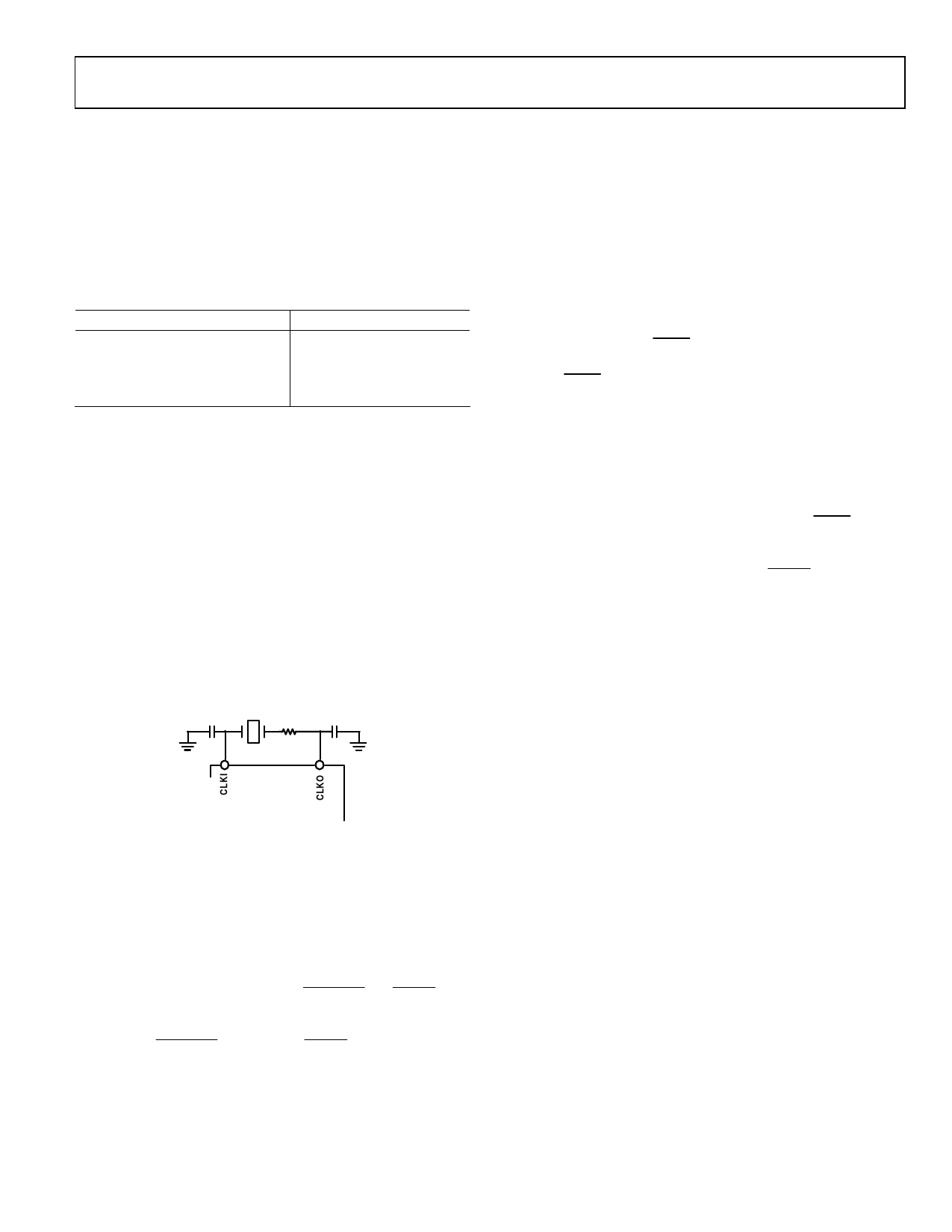
Clocking
The AD199x has two clock pins, CLKI and CLKO which are
used to configure the clocking scheme for the device. The
AD199x should be driven by a clock which is 256 × fS where fS
is the desired sampling rate. If a crystal is to be used as the
clock source it should be connected across the CLKI and
CLKO pins as shown in Figure 17. Crystal Connection The
values and type of capacitors used will be determined by the
crystal manufacturer. A square-wave clock source may be
connected directly to the CLKI pin. The logic levels of the
square wave should be compatible with those defined in the
Digital I/O section of the specifications page.
22pF
XTAL
47Ω
22pF
Figure 17. Crystal Connection
Output Transistor Non-Overlap Time
Ipsum lorum...
Power-up Considerations
Careful power-up is necessary when using the AD199x to
ensure correct operation and avoid possible latch-up issues. The
AD199x should be powered-up with RST/PDN and MUTE
held low until all the power supplies have stabilized. Once the
supplies have stabilized the AD199x can be brought out of reset
by bringing RST/PDN high and then MUTE can be brought
AD199x
high as required.
On/Off/Mute Pop Noise Suppression
The AD199x features pop suppression which is activated when
the part is reset or taken out of mute. The pop suppression is
achieved by pulsing the power outputs to bring the outputs of
the LC filter from 0V to mid-scale in a controlled fashion. This
feature eliminates unwanted transients on both the outputs and
the high voltage power supply.
Thermal Protection
The AD199x features thermal protection. When the die
temperature exceeds approximately 135°C the Thermal
Warning Error output (ERR1) is asserted. If the die temperature
exceeds approximately 150°C the Thermal Shutdown Error
output (ERR2) is asserted. If this occurs, the part shuts down to
prevent damage to the part. When the die temperature drops
below approximately 120°C both error outputs are negated and
the part returns to normal operation.
Over-current Protection
The AD199x features over current or short circuit protection. If
the current through any power transistors exceeds 4A the part
goes into mute and the Over-current error output (ERR0) is
asserted. This is a latched error and does not clear
automatically. To clear the error condition and restore normal
operation, the part must be either reset, or MUTE must be
asserted and negated.
Application Considerations
Good board layout and decoupling are vital for correct
operation of the AD199x. Due to the fact that the part switches
high currents there is the potential for large PVDD bounce each
time a transistor transitions. This can cause unpredictable
operation of the part. To avoid this potential problem, close
chip decoupling is essential. It is also recommended that the
decoupling capacitors are placed on the same side of the board
as the AD199x, and connected directly to the PVDD and
PGND pins. By placing the decoupling capacitors on the other
side of the board and decoupling through vias the effectiveness
of the decoupling is reduced. This is because vias have
inductive properties and therefore prevent very fast discharge
of the decoupling capacitors. Best operation is achieved with at
least one decoupling capacitor on each side of the AD199x, or
optionally two capacitors per side can be used to further reduce
the series resistance of the capacitor. If these decoupling
recommendations cannot be followed and decoupling through
vias is the only option, the vias should be made as large as
possible to increase surface area, thereby reducing inductance
and resistance.
Rev. PrA – 1/20/05 | Page 11 of 16
Share Link: 