ACPM-7822 Ver la hoja de datos (PDF) - Avago Technologies
Número de pieza
componentes Descripción
Fabricante
ACPM-7822 Datasheet PDF : 13 Pages
| |||
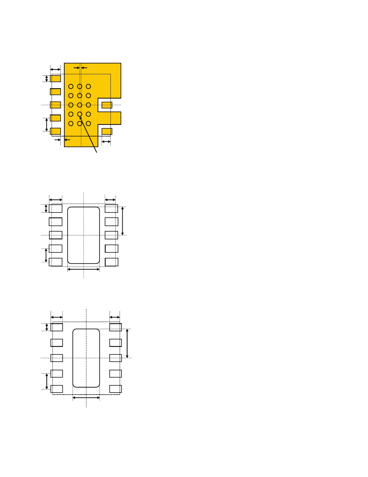
Metallization
0.1
0.6
0.4
0.85
0.25
0.5
Ø 0.3mm
on 0.6mm pitch
Solder Mask Opening
0.7
0.5
0.55
1.8
0.85
2.4
Solder Paste Stencil Aperture
0.6
0.5
0.4
1.6
0.85
2.0
6
PCB Design Guidelines
The recommended PCB land pattern is shown in figures
on the left side. The substrate is coated with solder mask
between the I/O and conductive paddle to protect the
gold pads from short circuit that is caused by solder
bleeding/bridging.
Stencil Design Guidelines
A properly designed solder screen or stencil is required
to ensure optimum amount of solder paste is deposited
onto the PCB pads.
The recommended stencil layout is shown here. Reducing
the stencil opening can potentially generate more voids.
On the other hand, stencil openings larger than 100% will
lead to excessive solder paste smear or bridging across
the I/O pads or conductive paddle to adjacent I/O pads.
Considering the fact that solder paste thickness will
directly affect the quality of the solder joint, a good choice
is to use laser cut stencil composed of 0.100mm(4mils) or
0.127mm(5mils) thick stainless steel which is capable of
producing the required fine stencil outline.
Share Link: 