AAT1157 Ver la hoja de datos (PDF) - Analog Technology Inc
Número de pieza
componentes Descripción
Fabricante
AAT1157 Datasheet PDF : 14 Pages
| |||
AAT1157
1MHz 1.2A Buck DC/DC Converter
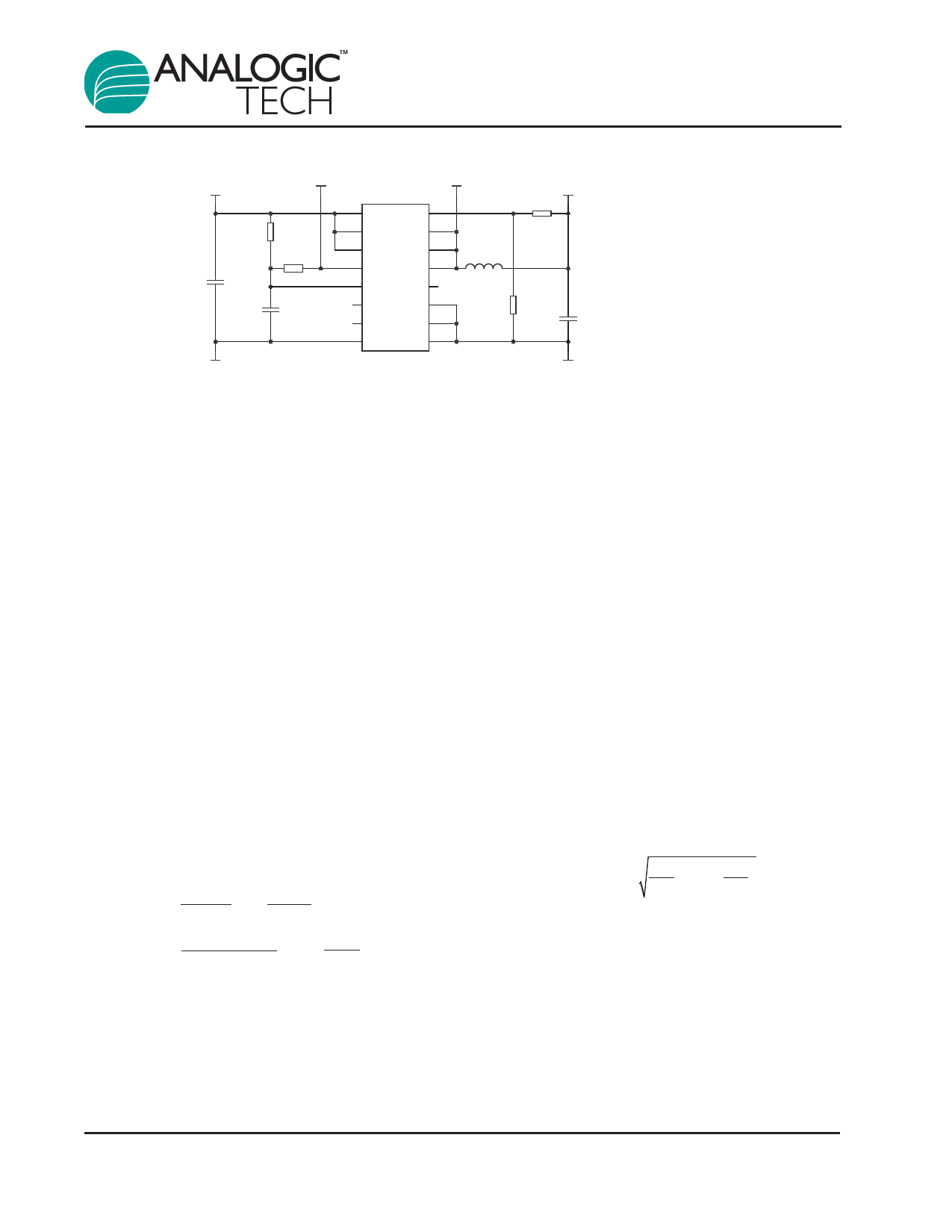
VIN+
C1
10µF
GND
Enable
R1
100
R2
100K
C2
0.1µF
U1
AAT1157
12
VP
4
FB
11
VP
15
LX
10
VP
14
LX
7
EN
13
LX
9
VCC
16
N/C
6
3
N/C PGND
8
2
N/C PGND
5
1
SGND PGND
LX
L1
3.0µH
R4
59.0k
VOUT+
R3
VOUT(V) R3 (kΩ)
0.8
19.6
0.9
29.4
1.0
39.2
1.1
49.9
1.2
59.0
1.3
68.1
1.4
78.7
1.5
88.7
1.8
118
C3-C4
2.0
137
2x 22µF
2.5
3.3
187
267
GND
C1 Murata 10µF 6.3V X5R GRM42-6X5R106K6.3
C3,C4 MuRata 22µF 6.3V GRM21BR60J226ME39L X5R 0805
L1 Sumida CDRH5D28-3R0NC
Figure 1: AAT1157 Evaluation Board Schematic
Lithium-Ion to 2.5V Converter.
Inductor
The output inductor should limit the ripple current to
330mA at the maximum input voltage. This match-
es the inductor current downslope with the fixed
internal slope compensation. For a 2.5V output and
the ripple set to a maximum input voltage of 4.2V,
the inductance value required to limit the ripple cur-
rent to 330mA is 3.0µH. From this calculated value,
a standard value can be selected.
Manufacturer's specifications list both the inductor
DC current rating, which is a thermal limitation, and
the peak current rating, which is determined by the
saturation characteristics. The inductor should not
show any appreciable saturation under normal load
conditions. Some inductors may meet the peak and
average current ratings yet result in excessive loss-
es due to a high DCR. Always consider the losses
associated with the DCR and its effect on the total
converter efficiency when selecting an inductor.
L
=
VOUT
∆IPP ⋅ F
⋅ ⎛⎝1
-
VOUT ⎞
VIN(MAX)⎠
=
2.5V
0.33A ⋅ 1MHz
⋅
⎛⎝1 -
2.5V ⎞
4.2V ⎠
= 3.07µH
For a maximum ripple current of 330mA, the peak
switch and inductor current at 1.2A is 1.365A. A stan-
dard value of 3.0µH can be used in this example. The
3.0µH Sumida series CDRH5D28 inductor has a
24mΩ maximum DCR and a 2.4A DC current rating.
Input Capacitor
The primary function of the input capacitor is to pro-
vide a low impedance loop for the edges of pulsed
current drawn by the AAT1157. A low ESR/ESL
ceramic capacitor is ideal for this function. To mini-
mize stray inductance, the capacitor should be
placed as closely as possible to the IC. This keeps
the high frequency content of the input current
localized, minimizing radiated and conducted EMI
while facilitating optimum performance of the
AAT1157. Ceramic X5R or X7R capacitors are
ideal for this function. The size required will vary
depending on the load, output voltage, and input
voltage source impedance characteristics. Values
range from 1µF to 10µF. The input capacitor RMS
current varies with the input voltage and the output
voltage. The equation for the RMS current in the
input capacitor is:
IRMS = IO ⋅
VO
VIN
⋅ ⎝⎛1 -
VO ⎞
VIN ⎠
The input capacitor RMS ripple current reaches a
maximum when VIN is two times the output volt-
age where it is approximately one half of the load
current. Losses associated with the input ceramic
capacitor are typically minimal and are not an
issue. The proper placement of the input capaci-
tor can be seen in the evaluation board layout (C1
in Figure 2).
8
1157.2005.11.1.4
Share Link: 