AAT1157 Ver la hoja de datos (PDF) - Analog Technology Inc
Número de pieza
componentes Descripción
Fabricante
AAT1157 Datasheet PDF : 14 Pages
| |||
AAT1157
1MHz 1.2A Buck DC/DC Converter
Pin Descriptions
Pin #
1, 2, 3
Symbol
PGND
4
FB
5
SGND
7
EN
6, 8, 16
9
10, 11, 12
13, 14, 15
EP
N/C
VCC
VP
LX
Function
Main power ground return pin. Connect to the output and input capacitor
return. (See board layout rules.)
Feedback input pin. This pin is connected to the converter output. It is used to
set the output of the converter to regulate to the desired value via an internal
resistive divider. For an adjustable output, an external resistive divider is con-
nected to this pin.
Signal ground. Connect the return of all small signal components to this pin.
(See board layout rules.)
Enable input pin. A logic high enables the converter; a logic low forces the
AAT1157 into shutdown mode reducing the supply current to less than 1µA.
The pin should not be left floating.
Not internally connected.
Bias supply. Supplies power for the internal circuitry. Connect to input power
via low pass filter with decoupling to SGND.
Input supply voltage for the converter power stage. Must be closely decoupled
to PGND.
Connect inductor to these pins. Switching node internally connected to the
drain of both high- and low-side MOSFETs.
Exposed paddle (bottom); connect to PGND directly beneath package.
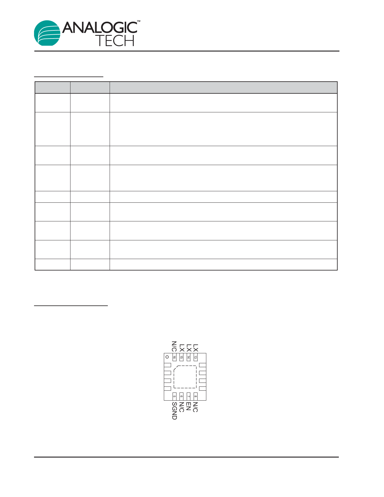
Pin Configuration
QFN33-16
(Top View)
PGND 1
PGND 2
PGND 3
FB 4
12 VP
11 VP
10 VP
9 VCC
2
1157.2005.11.1.4
Share Link: 