A8287 Ver la hoja de datos (PDF) - Allegro MicroSystems
Número de pieza
componentes Descripción
Fabricante
A8287 Datasheet PDF : 17 Pages
| |||
A8285/A8287
LNB Supply and Control Voltage Regulator
Application Information
Timing Considerations
The control sequence of the communication through the I2C
interface is composed of several steps in sequence:
1. Start Condition. Defined by a negative edge on the SDA
line, while SCL is high.
2. Address Cycle. 7 bits of address, plus 1 bit to indicate
read (1) or write (0), and an acknowledge bit. The first
five bits of the address are fixed as: 00010. The four
optional addresses, defined by the remaining two bits, are
selected by the ADD input. The address is transmitted
MSB first.
3. Data Cycles. 8 bits of data followed by an acknowledge
bit. Multiple data bytes can be read. Data is transmitted
MSB first.
4. Stop Condition. Defined by a positive edge on the SDA
line, while SCL is high.
Except to indicate a Start or Stop condition, SDA must be
stable while the clock is high. SDA can only be changed
while SCL is low. It is possible for the Start or Stop condition
to occur at any time during a data transfer. The A8285/A8287
always responds by resetting the data transfer sequence.
The Read/Write bit is used to determine the data transfer
direction. If the Read/Write bit is high, the master reads one
or more bytes from the A8285/A8287. If the Read/Write bit
is low, the master writes one byte to the A8285/A8287. Note
that multiple writes are not permitted. All write operations
must be preceded with the address.
The Acknowledge bit has two functions. It is used by the
master to determine if the slave device is responding to its
address and data, and it is used by the slave when the master
is reading data back from the slave. When the A8285/A8287
decodes the 7-bit address field as a valid address, it responds
by pulling SDA low during the ninth clock cycle.
During a data write from the master, the A8285/A8287 also
pulls SDA low during the clock cycle that follows the data
byte, in order to indicate that the data has been successfully
received. In both cases, the master device must release the
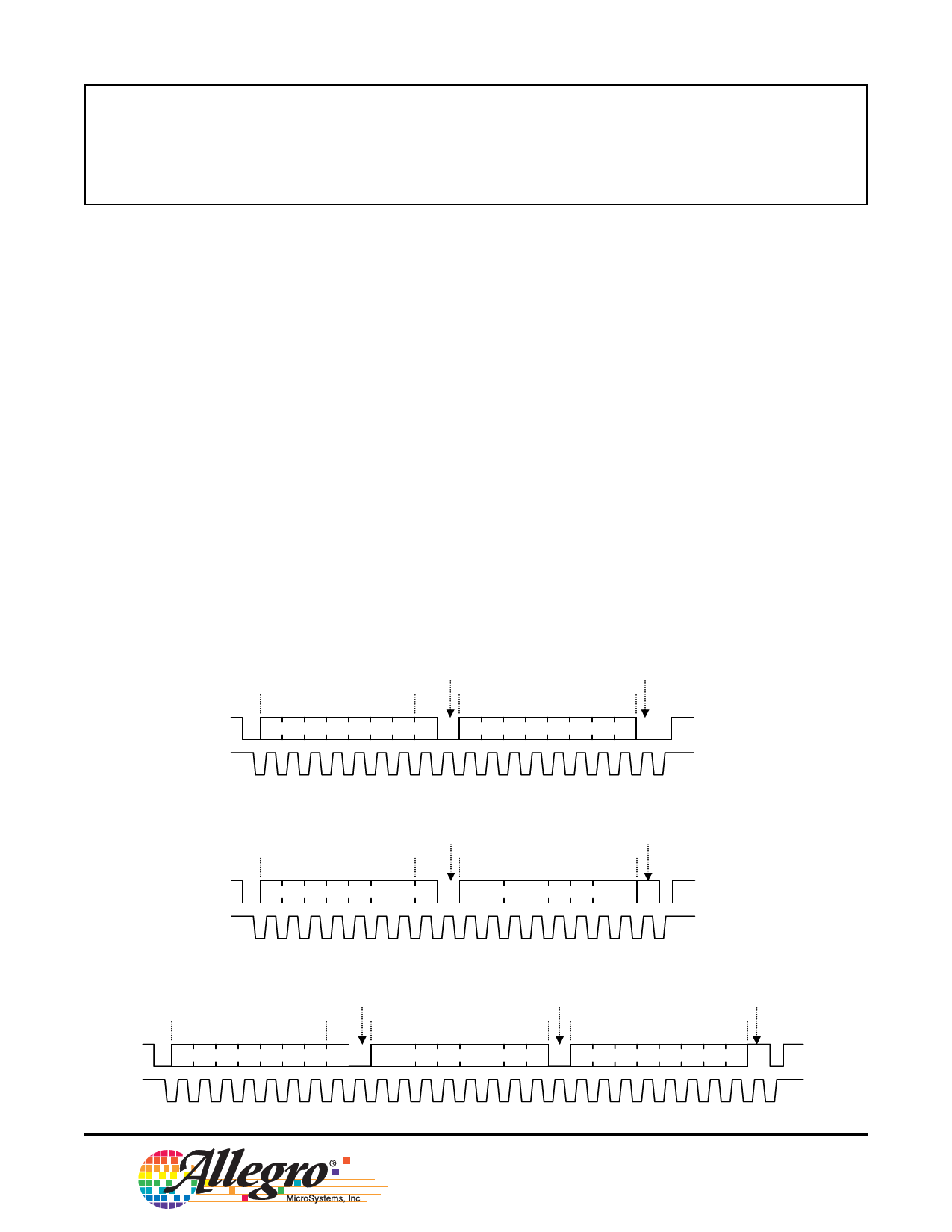
Writing to the Register
Start
Address
acknowledge
from LNBR
W
Control Data
acknowledge
from LNBR
Stop
SDA
0 0 0 1 0 A1 A0 0 AK D7 D6 D5 D4 D3 D2 D1 D0 AK
SCL
123456789
Reading One Byte from the Register
Start
Address
acknowledge
from LNBR
R
Status Data
no acknowledge
from master
Stop
SDA
0 0 0 1 0 A1 A0 1 AK D7 D6 D5 D4 D3 D2 D1 D0 NAK
SCL
123456789
Reading Multiple Bytes from the Register
acknowledge
from LNBR
Start
Address
R
Status Data
acknowledge
from master
Status Data
no acknowledge
from master
Stop
SDA
0 0 0 1 0 A1 A0 1 AK D7 D6 D5 D4 D3 D2 D1 D0 AK D7 D6 D5 D4 D3 D2 D1 D0 NAK
SCL
123456789
8
www.allegromicro.com
115 Northeast Cutoff, Box 15036
Worcester, Massachusetts 01615-0036 (508) 853-5000
Share Link: 