A40MX02(2014) Ver la hoja de datos (PDF) - Microsemi Corporation
Número de pieza
componentes Descripción
Fabricante
A40MX02 Datasheet PDF : 143 Pages
| |||
40MX and 42MX FPGA Families
D00
D01
D10
YD
Q OUT
D11
S0
S1
CLR
D00
D01
D10
YD
Q OUT
D11
S0
GATE
S1
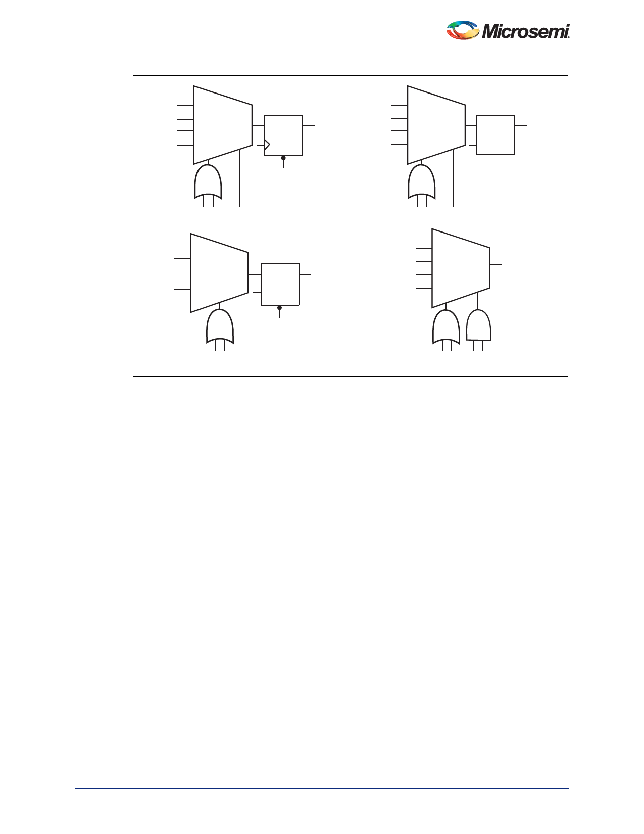
Up to 7-Input Function Plus D-Type Flip-Flop with Clear
D0
YD
Q OUT
D1
S
GATE
CLR
Up to 7-Input Function Plus Latch
D00
D01
D10
D11
S1
Y OUT
S0
Up to 4-Input Function Plus Latch with Clear
Up to 8-Input Function (Same as C-Module)
Figure 1-3 • 42MX S-Module Implementation
A42MX24 and A42MX36 devices contain D-modules, which are arranged around the periphery of the device. D-
modules contain wide-decode circuitry, providing a fast, wide-input AND function similar to that found in CPLD
architectures (Figure 1-4 on page 1-4). The D-module allows A42MX24 and A42MX36 devices to perform wide-
decode functions at speeds comparable to CPLDs and PALs. The output of the D-module has a programmable
inverter for active HIGH or LOW assertion. The D-module output is hardwired to an output pin, and can also be fed
back into the array to be incorporated into other logic.
Dual-Port SRAM Modules
The A42MX36 device contains dual-port SRAM modules that have been optimized for synchronous or asynchronous
applications. The SRAM modules are arranged in 256-bit blocks that can be configured as 32x8 or 64x4. SRAM
modules can be cascaded together to form memory spaces of user-definable width and depth. A block diagram of the
A42MX36 dual-port SRAM block is shown in Figure 1-5 on page 1-4.
The A42MX36 SRAM modules are true dual-port structures containing independent read and write ports. Each SRAM
module contains six bits of read and write addressing (RDAD[5:0] and WRAD[5:0], respectively) for 64x4-bit blocks.
When configured in byte mode, the highest order address bits (RDAD5 and WRAD5) are not used. The read and write
ports of the SRAM block contain independent clocks (RCLK and WCLK) with programmable polarities offering active
HIGH or LOW implementation. The SRAM block contains eight data inputs (WD[7:0]), and eight outputs (RD[7:0]),
which are connected to segmented vertical routing tracks.
The A42MX36 dual-port SRAM blocks provide an optimal solution for high-speed buffered applications requiring FIFO
and LIFO queues. The ACTgen Macro Builder within Microsemi's Designer software provides capability to quickly
design memory functions with the SRAM blocks. Unused SRAM blocks can be used to implement registers for other
user logic within the design.
1-3
Revision 12
Share Link: 